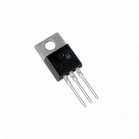
2N6394G ON Semiconductor, 2N6394G Datasheet - Page 2

2N6394G
Manufacturer Part Number
2N6394G
Description
THYRISTOR SCR 12A 50V TO-220AB
Manufacturer
ON Semiconductor
Datasheet
1.2N6395G.pdf
(5 pages)
Specifications of 2N6394G
Scr Type
Standard Recovery
Voltage - Off State
50V
Voltage - Gate Trigger (vgt) (max)
1.5V
Voltage - On State (vtm) (max)
2.2V
Current - On State (it (rms)) (max)
12A
Current - Gate Trigger (igt) (max)
30mA
Current - Hold (ih) (max)
50mA
Current - Off State (max)
10µA
Current - Non Rep. Surge 50, 60hz (itsm)
100A @ 60Hz
Operating Temperature
-40°C ~ 125°C
Mounting Type
Through Hole
Package / Case
TO-220-3 (Straight Leads)
Current - On State (it (rms) (max)
12A
Lead Free Status / RoHS Status
Lead free / RoHS Compliant
Current - On State (it (av)) (max)
-
Available stocks
Company
Part Number
Manufacturer
Quantity
Price
Part Number:
2N6394G
Manufacturer:
ON/安森美
Quantity:
20 000
†Indicates JEDEC Registered Data
2. Pulse Test: Pulse Width
ELECTRICAL CHARACTERISTICS
OFF CHARACTERISTICS
ON CHARACTERISTICS
DYNAMIC CHARACTERISTICS
†Peak Repetitive Forward or Reverse Blocking Current
(V
†Peak Forward On-State Voltage (Note 2) (I
†Gate Trigger Current (Continuous dc) (V
† Gate Trigger Voltage (Continuous dc) (V
† Holding Current (V
Turn‐On Time (I
Critical Rate-of-Rise of Off‐State Voltage Exponential
Gate Non-Trigger Voltage (V
Turn‐Off Time (V
Symbol
V
I
V
I
V
I
DRM
RRM
H
AK
130
125
120
105
100
DRM
RRM
TM
115
110
95
90
= Rated V
0
I
1.0
T(AV)
Parameter
Peak Repetitive Off State Forward Voltage
Peak Forward Blocking Current
Peak Repetitive Off State Reverse Voltage
Peak Reverse Blocking Current
Peak On State Voltage
Holding Current
DRM
TM
, AVERAGE ON‐STATE FORWARD CURRENT (AMPS)
D
= Rated V
= 12 A, I
2.0
or V
D
Figure 1. Current Derating
= 12 Vdc, Initiating Current = 200 mA, Gate Open)
= 30
RRM
3.0
GT
300 msec, Duty Cycle
, Gate Open)
DRM
D
= 40 mAdc, V
= 12 Vdc, R
)
60
Characteristic
4.0
(T
D
D
Voltage Current Characteristic of SCR
5.0
C
90
= CONDUCTION ANGLE
L
= 12 Vdc, R
= 12 Vdc, R
TM
D
= 25 C unless otherwise noted.)
= 100 Ohms, T
= Rated V
= 24 A Peak)
(I
6.0
TM
2%.
(V
= 12 A, I
180
D
L
L
DRM
= Rated V
= 100 Ohms)
http://onsemi.com
= 100 Ohms)
7.0
2N6394 Series
J
dc
)
(I
= 125 C)
R
TM
= 12 A, T
8.0
= 12 A, I
DRM
2
I
Reverse Avalanche Region
RRM
Anode -
, T
Reverse Blocking Region
T
J
J
8.0
6.0
4.0
2.0
T
J
at V
14
20
18
16
12
10
R
= 125 C)
= 125 C)
0
J
= 125 C
= 12 A)
= 25 C
0
RRM
Figure 2. Maximum On-State Power Dissipation
(off state)
= CONDUCTION ANGLE
1.0
I
I
T(AV)
DRM
on state
Symbol
dv/dt
V
V
V
2.0
, AVERAGE ON‐STATE CURRENT (AMPS)
I
GT
I
t
t
, I
GD
TM
GT
gt
H
q
RRM
= 30
+ Current
3.0
Forward Blocking Region
Min
60
0.2
I
H
-
-
-
-
-
-
-
-
-
-
4.0
V
TM
(off state)
Typ
90
1.7
5.0
0.7
6.0
1.0
15
35
50
-
-
-
5.0
I
DRM
Max
Anode +
2.0
2.2
1.5
2.0
at V
10
30
50
-
-
-
-
6.0
T
J
180
DRM
125 C
+ Voltage
7.0
Unit
V/ms
mA
mA
mA
mA
ms
ms
V
V
V
dc
8.0


