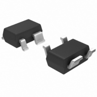
NESG2031M05-A CEL, NESG2031M05-A Datasheet

NESG2031M05-A
Specifications of NESG2031M05-A
Available stocks
Related parts for NESG2031M05-A
NESG2031M05-A Summary of contents
Page 1
... Pb Free Available (-A) DESCRIPTION NEC's NESG2031M05 is fabricated using NECʼs high voltage Silicon Germanium process (UHS2-HV), and is designed for a wide range of applications including low noise amplifiers, medium power amplifiers, and oscillators. NECʼs low profile, flat lead style M05 Package provides high frequency performance for compact wireless designs. ...
Page 2
... SYMBOLS V 13 j-c V 5 175 ORDERING INFORMATION °C 150 PART NUMBER °C -65 to +150 NESG2031M05-T1 NESG2031M05-T1-A 3 kpcs/reel • Pb Free (T = 25ºC) A 125 150 (°C) A 0.0001 0.9 1.0 (V) BE NESG2031M05 PARAMETERS UNITS Junction to Case Resistance °C/W QUANTITY SUPPLY FORM 3 kpcs/reel • Pin 3 (Collector), Pin 4 (Emitter) face the perforation • ...
Page 3
... DC CURRENT GAIN vs. COLLECTOR CURRENT 1 000 100 10 0 Collector Current, l (mA 25ºC) A 0.9 1.0 ( 000 100 100 100 NESG2031M05 COLLECTOR CURRENT vs. COLLECTOR TO EMITTER VOLTAGE 35 µ 200 A µ 180 A 30 µ 160 A µ 25 140 A µ 120 A 20 µ 100 A µ µ µ µ ...
Page 4
... S21e 0 Frequency, f (GHz) INSERTION POWER GAIN, MAG, MSG vs. FREQUENCY 40 35 MSG 30 MAG 21e 0 Frequency, f (GHz 25ºC) A 100 100 100 NESG2031M05 GAIN BANDWIDTH PRODUCT vs. COLLECTOR CURRENT GHz 100 Collector Current, l (mA) C INSERTION POWER GAIN, MAG, MSG vs. FREQUENCY MSG 30 MAG S21e 0 100 Frequency, f (GHz) INSERTION POWER GAIN, MAG, MSG vs ...
Page 5
... INSERTION POWER GAIN, MAG, MSG vs. COLLECTOR CURRENT GHz 25 MSG 21e Collector Current 25ºC) A 100 (mA) C 100 (mA) C MAG 100 (mA) C NESG2031M05 INSERTION POWER GAIN, MAG, MSG vs. COLLECTOR CURRENT GHz 25 MSG MAG 21e 100 Collector Current, I (mA) C INSERTION POWER GAIN, MAG, MSG vs. COLLECTOR CURRENT MSG GHz ...
Page 6
... INSERTION POWER GAIN, MAG, MSG vs. COLLECTOR CURRENT GHz 25 20 MAG 21e Collector Current 25ºC) A 100 (mA) MAG 100 (mA) 100 (mA) NESG2031M05 INSERTION POWER GAIN, MAG, MSG vs. COLLECTOR CURRENT MSG GHz 21e Collector Current, I (mA) C INSERTION POWER GAIN, MAG, MSG vs. COLLECTOR CURRENT GHz 25 MSG ...
Page 7
... COLLECTOR CURRENT Collector Current 25º (dBm (dBm GHz 0 100 (mA) C NESG2031M05 OUTPUT POWER, COLLECTOR CUR- RENT vs. INPUT POWER GHz (RF OFF out -20 -15 - Input Power, P (dBm) in NOISE FIGURE, ASSOCIATED GAIN vs. COLLECTOR CURRENT GHz 100 Collector Current, I (mA) C NOISE FIGURE, ASSOCIATED GAIN vs. COLLECTOR CURRENT 6 5 ...
Page 8
... Collector Current 25º GHz 0 100 (mA 5.2 GHz 0 100 (mA GHz 0 100 (mA) NESG2031M05 NOISE FIGURE, ASSOCIATED GAIN vs. COLLECTOR CURRENT 5.2 GHz 100 Collector Current, I (mA) C NOISE FIGURE, ASSOCIATED GAIN vs. COLLECTOR CURRENT GHz 100 Collector Current, I (mA) C NOISE FIGURE, ASSOCIATED GAIN vs. COLLECTOR CURRENT ...
Page 9
... NESG2031M05 +90º +135º +45º +0º -135º -45º -90º MAG ANG 0.961 -12.14 0.109 0.917 -22 ...
Page 10
... NESG2031M05 +90º +135º +45º +0º -135º -45º -90º MAG 22 MAG ANG (dB) 0.900 -20.46 ...
Page 11
... OUTLINE DIMENSIONS (Units in mm) PACKAGE OUTLINE M05 FLAT LEAD 4-PIN THIN TYPE SUPER MINIMOLD 2.05±0.1 1.25±0.1 3 2.0 ±0.1 4 +0.1 0.30 -0.05 0.59±0.05 PIN CONNECTIONS 1. Base 2. Emitter 3. Collector 4. Emitter 2 0.65 1.30 0.65 1 +0.1 0.11 -0.05 NESG2031M05 ...
Page 12
... C CBPKG 0 C CEPKG 0.8 C BEPKG 4e- 0 1.11 MODEL TEST CONDITIONS 1.3 Frequency: 0 GHz 5.2 Bias: V Date: 09/2003 0 1 NESG2031M05 Collecto r NESG2031M05 0.13 pF 0.01 pF 0.03 pF 0.9 nH BPKG 1.0 nH CPKG 0.19 nH EPKG = Business Partner of NEC Compound Semiconductor Devices, Ltd. ...
Page 13
... CAS numbers and other limited information may not be available for release event shall CELʼs liability arising out of such information exceed the total purchase price of the CEL part(s) at issue sold by CEL to customer on an annual basis. ...


