NESG2030M04-A CEL, NESG2030M04-A Datasheet
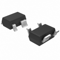
TRANS NPN 2GHZ SOT-343

NESG2030M04-A

Manufacturer Part Number
NESG2030M04-A
Description
TRANS NPN 2GHZ SOT-343
Manufacturer
CEL
Datasheet

Specifications of NESG2030M04-A

Transistor Type
NPN
Voltage - Collector Emitter Breakdown (max)
2.3V
Frequency - Transition
60GHz
Noise Figure (db Typ @ F)
0.9dB ~ 1.1dB @ 2GHz
Gain
16dB
Power - Max
80mW
Dc Current Gain (hfe) (min) @ Ic, Vce
200 @ 5mA, 2V
Current - Collector (ic) (max)
35mA
Mounting Type
Surface Mount
Package / Case
SC-70-4, SC-82-4, SOT-323-4, SOT-343
Continuous Collector Current
35 mA
Emitter- Base Voltage Vebo
1.2 V
Maximum Operating Temperature
+ 150 C
Mounting Style
SMD/SMT
Power Dissipation
80 mW
Lead Free Status / RoHS Status
Lead free / RoHS Compliant
Lead Free Status / RoHS Status
Lead free / RoHS Compliant, Lead free / RoHS Compliant
ELECTRICAL CHARACTERISTICS
Notes:
DESCRIPTION
NEC's NESG2030M04 is fabricated using NEC's state-of-the-art SiGe, wafer process. With a typical transition frequency of
60 GHz the NESG2030M04 is usable in applications from 100 MHz to over 10 GHz. Maximum DC current input of 35 mA provides
a device with a usable current range of 250 μA to 25 mA. The NESG2030M04 provides excellent low voltage/low current performance.
NEC's new low profile/flat lead style "M04" package is ideal for today's portable wireless applications. The NESG2030M04 is an ideal
choice for LNA and oscillator requirements in all mobile communication systems.
Date Published: June 22, 2005
• SiGe TECHNOLOGY:
• LOW NOISE FIGURE:
• HIGH MAXIMUM STABLE GAIN:
• NEW LOW PROFILE M04 PACKAGE:
FEATURES
f
NF = 0.9 dBm at 2 GHz
MSG = 20 dB at 2 GHz
SOT-343 footprint, with a height of only 0.59 mm
Flat lead style for better RF performance
T
= 60 GHz Process
1. Electronic Industrial Association of Japan.
2. Pulsed measurement, pulse width ≤ 350 μs, duty cycle ≤ 2 %.
3. Collector to base capacitance is measured by capacitance meter (automatic balance bridge method) when emitter pin is connected to
4. MSG = S
SYMBOLS
the guard pin.
|S
MSG
OIP
P
I
I
h
C
CBO
EBO
NF
G
21E
1dB
FE
re
a
3
|
2
S
The information in this document is subject to change without notice. Before using this document, please confirm
that this is the latest version.
21
12
Collector Cutoff Current at V
Emitter Cutoff Current at V
DC Current Gain
Reverse Transfer Capacitance
Noise Figure at V
Associated Gain at V
Maximum Stable Gain
Insertion Power Gain at V
Output Power at 1 dB compression point
V
Third Order Intercept Point, V
CE
= 2 V, I
NPN SiGe HIGH FREQUENCY TRANSISTOR
C
= 20 mA, f = 2 GHz
PARAMETERS AND CONDITIONS
2
EIAJ
CE
at V
= 2 V, I
CE
PACKAGE OUTLINE
1
4
CE
REGISTERED NUMBER
at V
= 2 V, I
PART NUMBER
= 2 V, I
CE
(T
EB
C
CE
A
CB
= 2 V, I
= 5 mA, f = 2 GHz, Z
= 0.5 V, I
CE
= 25°C)
3
= 2 V, I
= 5V, I
C
at V
C
= 2 V, I
= 5 mA, f = 2 GHz, Z
= 5 mA
C
CB
= 20 mA, f = 2 GHz
E
C
C
= 2 V, I
= 0
C
= 20 mA, f = 2 GHz
= 0
= 20 mA, f = 2 GHz
E
= 0 mA, f = 1 GHz
IN
= Z
S
= Z
OPT
M04
OPT
NESG2030M04
NPN SiGe RF TRANSISTOR
UNITS
GHz
dBm
dBm
nA
nA
pF
dB
dB
dB
MIN
200
18
16
NESG2030M04
2SC5761
M04
TYP
0.17
0.9
16
20
18
12
22
MAX
0.22
200
200
400
1.1

Related parts for NESG2030M04-A

NESG2030M04-A Summary of contents

Page 1

... NEC's NESG2030M04 is fabricated using NEC's state-of-the-art SiGe, wafer process. With a typical transition frequency of 60 GHz the NESG2030M04 is usable in applications from 100 MHz to over 10 GHz. Maximum DC current input provides a device with a usable current range of 250 μ mA. The NESG2030M04 provides excellent low voltage/low current performance. ...

Page 2

... R th j-c V 2.3 V 1.2 ORDERING INFORMATION mA 35 PART NUMBER mW 80 NESG2030M04 °C 150 NESG2030M04-T2 -65 to +150 °C ORDERING INFORMATION (Pb-Free) PART NUMBER NESG2030M04-A NESG2030M04-T2 25°C) A 190 μa 160 μa 130 μa 100 μa 70 μa 40 μ μ (V) CE 100 NESG2030M04 PARAMETERS UNITS Junction to Case Resistance ° ...

Page 3

... THIRD ORDER INTERMODULATION DISTORTION vs. OUTPUT POWER Output Power (each tone 25°C) A 100 (mA 100 (mA GHz offset = 1 MHz 15 20 (mA) out NESG2030M04 MAXIMUM STABLE GAIN, INSERTION POWER GAIN vs. COLLECTOR CURRENT GHz 25 MSG 21e Collector Current, I (mA) C OUTPUT POWER, COLLECTOR CURRENT vs. INPUT POWER GHz mA(RF OFF out 10 ...

Page 4

... NOISE FIGURE AND ASSOCIATED GAIN vs. COLLECTOR CURRENT GHz Collector Current, I (mA 25°C) A NOISE FIGURE AND ASSOCIATED GAIN vs. COLLECTOR CURRENT 2.5 GHz 100 1 NOISE FIGURE AND ASSOCIATED GAIN vs. COLLECTOR CURRENT GHz 100 100 NESG2030M04 100 Collector Current, l (mA 100 Collector Current, l (mA) C ...

Page 5

... PIN CONNECTIONS 29.4 0.17 1. Emitter 34.5 0.16 2. Collector 40.4 0.16 3. Emitter 4. Base 47.1 0.16 63.0 0.15 81.1 0.15 NESG2030M04 (CONT Γ MIN A OPT (dB) (dB) MAG ANG Rn/ 1.26 18.16 0.064 90.1 1.27 17.40 0.072 106.5 1.28 16 ...

Page 6

... NESG2030M04 NESG2030M04 Vc = 2.000 5.000 mA +90° +120° +60° +150° +30° +180° +0° -150° -30° -120° -60° -90° 0.100 to 12.000GHz by 0.100 ...

Page 7

... NESG2030M04 +90° +120° +60° +150° +30° +180° +0° -150° -30° 0.100 to 12.000GHz by 0.100 -120° -60° -90° S MAG ...

Page 8

... NESG2030M04 +90° +90° +120° +120° +60° +60° +150° +150° +30° +30° +180° +180° +0° +0° 0.100 to 12.000GHz by 0.100 -150° ...

Page 9

... NESG2030M04 NONLINEAR MODEL SCHEMATIC Base BJT NONLINEAR MODEL PARAMETERS Parameters Q1 Parameters IS 2.42e-13 MJC BF 382 XCJC NF 1.025 CJS VAF 87 VJS IKF 100 MJS ISE 5.2e- 2.806 TF BR 15.7 XTF NR 1.02 VTF VAR 1.307 ITF IKR 0.037 PTF ISC 9e- 2.194 EG RE 2.2 XTB ...

Page 10

... CAS numbers and other limited information may not be available for release event shall CEL’s liability arising out of such information exceed the total purchase price of the CEL part(s) at issue sold by CEL to customer on an annual basis. ...

Related keywords