NE662M04-A CEL, NE662M04-A Datasheet
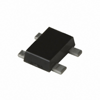
TRANSISTOR NPN 2GHZ M04

NE662M04-A

Manufacturer Part Number
NE662M04-A
Description
TRANSISTOR NPN 2GHZ M04
Manufacturer
CEL
Datasheet

Specifications of NE662M04-A

Transistor Type
NPN
Voltage - Collector Emitter Breakdown (max)
3.3V
Frequency - Transition
25GHz
Noise Figure (db Typ @ F)
1.1dB ~ 1.5dB @ 2GHz
Gain
20dB
Power - Max
115mW
Dc Current Gain (hfe) (min) @ Ic, Vce
50 @ 5mA, 2V
Current - Collector (ic) (max)
35mA
Mounting Type
Surface Mount
Package / Case
M04
Dc Collector/base Gain Hfe Min
70
Mounting Style
SMD/SMT
Configuration
Single
Transistor Polarity
NPN
Maximum Operating Frequency
25 GHz
Collector- Emitter Voltage Vceo Max
3.3 V
Emitter- Base Voltage Vebo
1.5 V
Continuous Collector Current
0.035 A
Power Dissipation
0.115 W
Lead Free Status / RoHS Status
Lead free / RoHS Compliant
Lead Free Status / RoHS Status
Lead free / RoHS Compliant, Lead free / RoHS Compliant
Other names
NE662M04-T2-A
• HIGH GAIN BANDWIDTH: f
• LOW NOISE FIGURE: NF = 1.1 dB at 2 GHz
• HIGH MAXIMUM STABLE GAIN: 20 dB at f = 2 GHz
• NEW LOW PROFILE M04 PACKAGE:
DESCRIPTION
FEATURES
NEC's NE662M04 is fabricated using NEC's UHS0 25 GHz f
NE662M04 is usable in applications from 100 MHz to 10 GHz. The NE662M04 provides excellent low voltage/low current
performance.
NEC's new low profile/flat lead style "M04" package is ideal for today's portable wireless applications. The NE662M04 is an ideal choice
for LNA and oscillator requirements in all mobile communication systems.
ELECTRICAL CHARACTERISTICS
Date Published: June 22, 2005
Notes:
• SOT-343 footprint, with a height of just 0.59 mm
• Flat Lead Style for better RF performance
1. Electronic Industrial Association of Japan.
2. Pulsed measurement, pulse width ≤ 350 µs, duty cycle ≤ 2 %.
3. Capacitance is measured by capacitance meter (automatic balance bridge method) when emitter pin is connected to the guard pin.
4. MAG =
5. MSG = S
SYMBOLS
|S
MAG
MSG
P
I
I
Cre
h
CBO
EBO
NF
IP
21E
f
1dB
FE
T
3
|
2
S
S
S
21
12
21
12
The information in this document is subject to change without notice. Before using this document, please confirm
that this is the latest version.
(
Collector Cutoff Current at V
Emitter Cutoff Current at V
Forward Current Gain
Gain Bandwidth at V
Maximum Available Power Gain
Maximum Stable Gain
Insertion Power Gain at V
Noise Figure at V
Output Power at 1 dB compression point at
V
Third Order Intercept Point at V
Feedback Capacitance
K-
CE
(K
= 2 V, I
2
-1)
T
)
C
= 25 GHz
= 20 mA, f = 2 GHz
PARAMETERS AND CONDITIONS
EIAJ
CE
CE
= 2 V, I
2
1
PACKAGE OUTLINE
5
FREQUENCY TRANSISTOR
3
at V
REGISTERED NUMBER
= 3 V, I
at V
PART NUMBER
at V
CE
(T
EB
CE
C
CE
A
CB
= 2 V, I
CB
= 5 mA, f = 2 GHz, Z
= 1 V, I
NPN SILICON HIGH
= 25°C)
= 2 V, I
C
= 2 V, I
= 5V, I
CE
= 2 V, I
4
= 30 mA, f = 2 GHz
at V
= 2 V, I
C
C
CE
C
= 20 mA, f = 2 GHz
E
C
= 0
C
= 5 mA
= 0
= 20 mA, f = 2 GHz
= 2 V, I
= 0, f = 1 MHz
C
= 20 mA, f = 2 GHz
T
wafer process. With a typical transition frequency of 25 GHz the
C
= 20 mA, f = 2 GHz
IN
= Z
OPT
M04
NPN SILICON RF TRANSISTOR
UNITS
GHz
dBm
NE662M04
nA
nA
dB
dB
dB
dB
pF
MIN
50
20
14
NE662M04
2SC5508
M04
TYP
0.18
1.1
70
25
20
20
17
11
22
MAX
0.24
200
200
100
1.5

Related parts for NE662M04-A

NE662M04-A Summary of contents

Page 1

... NE662M04 is usable in applications from 100 MHz to 10 GHz. The NE662M04 provides excellent low voltage/low current performance. NEC's new low profile/flat lead style "M04" package is ideal for today's portable wireless applications. The NE662M04 is an ideal choice for LNA and oscillator requirements in all mobile communication systems. ...

Page 2

... C = -5.0 0.8 0.9 -2.0 1.0 1.5 1.8 1.9 2.0 2.5 2.0 5.0 THERMAL RESISTANCE 0 Junction to Case Resistance -5.0 Junction to Ambient Resistance -2.0 NE662M04 (T = 25˚ Γ Γ Γ Γ Γ MIN A OPT (dB) (dB) MAG ANG 3 mA 0.78 21.4 0.26 31.7 0.80 20 ...

Page 3

... V CE 25.0 5.00 20.0 4.00 15.0 3.00 10.0 2.00 5.0 1.00 0.0 0.00 100 NE662M04 NOISE FIGURE AND ASSOCIATED GAIN vs. FREQUENCY 2V Frequency, f (GHz) NOISE FIGURE AND ASSOCIATED GAIN vs. COLLECTOR CURRENT 30 ...

Page 4

... BE NE662M04 DC CURRENT GAIN vs. COLLECTOR CURRENT Collector Current, l (mA) C COLLECTOR CURRENT vs. COLLECTOR TO EMITTER VOLTAGE 355 µA 305 µA 255 µA 205 µA 155 µA 105 µ µ µA ...

Page 5

... GAIN vs. COLLECTOR CURRENT 30. GHz 25.00 MSG 20. 15.00 10.00 5.00 0. Collector Current 25˚ MAG 10 MAG 100 (mA) NE662M04 FORWARD INSERTION GAIN AND MAXIMUM AVAILABLE GAIN vs. FREQUENCY MSG MAG Frequency, f (GHz) MAXIMUM STABLE GAIN, INSERTION POWER GAIN, MAXIMUM AVAILABLE GAIN vs. COLLECTOR CURRENT 30. GHz 25.00 MAG 20 ...

Page 6

... PIN CONNECTIONS 1. Emitter 2. Collector 3. Emitter 4. Base ORDERING INFORMATION (Solder Contains Lead) PART NUMBER QUANTITY NE662M04-T2 3000 ORDERING INFORMATION (Pb-Free) PART NUMBER QUANTITY NE662M04-T2-A 3000 0.65 1.30 0.65 +0.1 0.11 -0.08 PACKAGING Tape & Reel PACKAGING Tape & Reel NE662M04 ...

Page 7

... NE662M04 90˚ 120˚ 60˚ 150˚ 30˚ 0.1 GHz S 12 0˚ GHz 21 18 GHz S 21 -150˚ -30˚ 0.1 GHz -120˚ ...

Page 8

... NE662M04 90˚ 120˚ 60˚ 150˚ S 30˚ GHz 0˚ 0.1 GHz 0.1 GHz GHz -150˚ -30˚ -120˚ ...

Page 9

... NE662M04 90˚ 120˚ 60˚ GHz 150˚ 30˚ 0˚ 0.1 GHz 0.1 GHz GHz -150˚ -30˚ -120˚ ...

Page 10

... NE662M04 NONLINEAR MODEL SCHEMATIC Base BJT NONLINEAR MODEL PARAMETERS Parameters Q1 Parameters IS 1.6e-16 MJC BF 111 XCJC NF 1.02 CJS VAF 23 VJS IKF 0.38 MJS ISE 1e XTF NR 1.02 VTF VAR 2.5 ITF IKR 0.1 PTF ISC 3e- 1. 0.77 XTB RB 3.5 XTI RBM 20 KF IRB 1 ...

Page 11

... CAS numbers and other limited information may not be available for release event shall CEL’s liability arising out of such information exceed the total purchase price of the CEL part(s) at issue sold by CEL to customer on an annual basis. ...

Related keywords