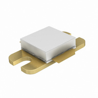
BLF6G20-45,112 NXP Semiconductors, BLF6G20-45,112 Datasheet - Page 5

BLF6G20-45,112
Manufacturer Part Number
BLF6G20-45,112
Description
TRANSISTOR BASESTATION SOT-608A
Manufacturer
NXP Semiconductors
Datasheet
1.BLF6G20-45135.pdf
(12 pages)
Specifications of BLF6G20-45,112
Package / Case
SOT-608A
Transistor Type
LDMOS
Frequency
1.8GHz
Gain
19.2dB
Voltage - Rated
65V
Current Rating
13A
Current - Test
360mA
Voltage - Test
28V
Power - Output
2.5W
Configuration
Single
Transistor Polarity
N-Channel
Resistance Drain-source Rds (on)
0.2 Ohms
Drain-source Breakdown Voltage
65 V
Gate-source Breakdown Voltage
13 V
Continuous Drain Current
13 A
Maximum Operating Temperature
+ 225 C
Mounting Style
SMD/SMT
Minimum Operating Temperature
- 65 C
Lead Free Status / RoHS Status
Lead free / RoHS Compliant
Noise Figure
-
Lead Free Status / RoHS Status
Lead free / RoHS Compliant, Lead free / RoHS Compliant
Other names
934060065112
BLF6G20-45
BLF6G20-45
BLF6G20-45
BLF6G20-45
NXP Semiconductors
8. Test information
BLF6G20-45_BLF6G20S-45_2
Product data sheet
Fig 4.
Fig 6.
(dB)
V
G
GG
p
25
23
21
19
17
15
0
V
MHz; carrier spacing 5 MHz.
2-carrier W-CDMA power gain and drain
efficiency as functions of average load power;
typical values
See
Test circuit for operation at 1805 MHz and 1880 MHz
input
50
DS
= 28 V; I
C3
Table 8
3
C4
for list of components.
Dq
= 360 mA; f
6
C5
R1
9
1
= 1840.5 MHz; f
C6
12
P
001aah548
G
L(AV)
C1
D
p
C2
(W)
Rev. 02 — 25 August 2008
15
2
= 1845.5
50
40
30
20
10
0
(%)
D
BLF6G20-45; BLF6G20S-45
Fig 5.
ACPR
(dBc)
20
30
40
50
60
0
V
MHz; carrier spacing 5 MHz.
2-carrier W-CDMA adjacent power channel
ratio as function of average load power;
typical values
C8
DS
= 28 V; I
C9
3
Dq
C7
= 360 mA; f
C10
6
C11
Power LDMOS transistor
C16
C15
9
1
= 1840.5 MHz; f
C12
© NXP B.V. 2008. All rights reserved.
12
P
C13
001aah549
L(AV)
output
50
(W)
001aah550
15
2
C14
= 1845.5
V
DD
5 of 12


