MRF5S9100NR1 Freescale Semiconductor, MRF5S9100NR1 Datasheet
MRF5S9100NR1
Specifications of MRF5S9100NR1
Available stocks


Related parts for MRF5S9100NR1

MRF5S9100NR1 Summary of contents
Page 1
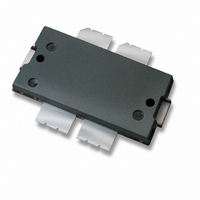
... Freescale Semiconductor Technical Data Replaced by MRF5S9100NR1/NBR1. There are no form, fit or function changes with this part replacement. N suffix added to part number to indicate transition to lead - free terminations. RF Power Field Effect Transistors N - Channel Enhancement - Mode Lateral MOSFETs Designed for broadband commercial and industrial applications with frequencies up to 1000 MHz ...
Page 2
... Vdc — 3.7 — Vdc — 0.21 0.3 Vdc — 7 — S — 70 — pF — 2.2 — Avg CDMA 880 MHz, out 18 19.5 — — % — dBc — Device Data Freescale Semiconductor ...
Page 3
... Chip Capacitors C9, C10 5.1 pF Chip Capacitors C13 470 mF Electrolytic Capacitor C14, C15 22 mF Tantalum Capacitors C16, C17, C19 0.56 mF Chip Capacitors C20, C21 47 mF Tantalum Capacitors C22 100 mF Electrolytic Capacitor L1 7.15 nH Inductor Inductor RF Device Data Freescale Semiconductor C18 Z10 DUT Z10 Z12 ...
Page 4
... Freescale has begun the transition of marking Printed Circuit Boards (PCBs) with the Freescale Semiconductor signature/logo. PCBs may have either Motorola or Freescale markings during the transition period. These changes will have no impact on form, fit or function of the current product. Figure 2. MRF5S9100MR1(MBR1) Test Circuit Component Layout ...
Page 5
... Vdc 880 MHz 880.1 MHz DD Two −Tone Measurements, 100 kHz Tone Spacing 16 0 OUTPUT POWER (WATTS) PEP out Figure 5. Two - Tone Power Gain versus Output Power RF Device Data Freescale Semiconductor TYPICAL CHARACTERISTICS G ps η Vdc (Avg.), I = 950 mA DD out DQ N−CDMA IS−95 (Pilot, Sync, Paging, Traffic ...
Page 6
... Pulsed CW, 8 μsec(on), 1 msec(off) Center Frequency = 880 MHz INPUT POWER (dBm) in Input Power −30 −35 −40 −45 −50 −55 −60 −65 −70 −75 −80 100 120 140 160 180 200 T , JUNCTION TEMPERATURE (° for MTTF in a particular application Device Data Freescale Semiconductor 38 220 ...
Page 7
... MHz f = 865 MHz Figure 12. Series Equivalent Source and Load Impedance RF Device Data Freescale Semiconductor Z load f = 865 MHz f = 895 MHz Z source = 5 Ω Vdc 950 mA Avg out source load MHz Ω Ω 865 3.0 - j1.8 1.4 - j0.7 880 2.8 - j1.9 1.5 - j0.6 895 2 ...
Page 8
... E5 .346 .350 8.79 8.89 F .025 BSC 0.64 BSC b1 .164 .170 4.17 4.32 c1 .007 .011 0.18 0.28 e .106 BSC 2.69 BSC aaa .004 0.10 STYLE 1: PIN 1. DRAIN 2. DRAIN 3. GATE 4. GATE 5. SOURCE RF Device Data Freescale Semiconductor ...
Page 9
... RF Device Data Freescale Semiconductor MRF5S9100MR1 MRF5S9100MBR1 9 ...
Page 10
... MRF5S9100MR1 MRF5S9100MBR1 10 RF Device Data Freescale Semiconductor ...
Page 11
... RF Device Data Freescale Semiconductor MRF5S9100MR1 MRF5S9100MBR1 11 ...
Page 12
... Freescale Semiconductor product could create a situation where personal injury or death may occur. Should Buyer ...