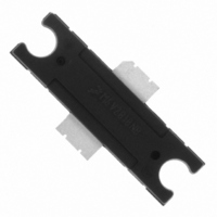
MRF6V2010NBR5 Freescale Semiconductor, MRF6V2010NBR5 Datasheet - Page 6

MRF6V2010NBR5
Manufacturer Part Number
MRF6V2010NBR5
Description
MOSFET RF N-CH 50V TO-272-2
Manufacturer
Freescale Semiconductor
Datasheet
1.MRF6V2010NBR5.pdf
(21 pages)
Specifications of MRF6V2010NBR5
Transistor Type
N-Channel
Frequency
220MHz
Gain
23.9dB
Voltage - Rated
110V
Current Rating
2.5mA
Current - Test
30mA
Voltage - Test
50V
Power - Output
10W
Package / Case
TO-272-2
Configuration
Single
Drain-source Breakdown Voltage
110 V
Gate-source Breakdown Voltage
- 5 V or 10 V
Maximum Operating Temperature
+ 200 C
Minimum Operating Temperature
- 65 C
Mounting Style
SMD/SMT
Transistor Polarity
N-Channel
Channel Type
N
Channel Mode
Enhancement
Drain Source Voltage (max)
110V
Output Power (max)
10W
Power Gain (typ)@vds
23.9dB
Frequency (min)
10MHz
Frequency (max)
450MHz
Package Type
TO-272 EP
Pin Count
3
Input Capacitance (typ)@vds
16.3@50VpF
Output Capacitance (typ)@vds
7.3@50VpF
Reverse Capacitance (typ)
0.13@50VpF
Operating Temp Range
-65C to 225C
Drain Efficiency (typ)
62%
Mounting
Surface Mount
Mode Of Operation
CW
Number Of Elements
1
Vswr (max)
10
Screening Level
Military
Drain Source Voltage Vds
110V
Rf Transistor Case
TO-272
Filter Terminals
SMD
Output Power Pout
10W
Peak Reflow Compatible (260 C)
Yes
Rohs Compliant
Yes
Gate-source Voltage
10V
Leaded Process Compatible
Yes
Operating Frequency Max
220MHz
Lead Free Status / RoHS Status
Lead free / RoHS Compliant
Noise Figure
-
Lead Free Status / Rohs Status
Lead free / RoHS Compliant
Other names
MRF6V2010NBR5TR
Available stocks
Company
Part Number
Manufacturer
Quantity
Price
Company:
Part Number:
MRF6V2010NBR5
Manufacturer:
FREESCALE
Quantity:
418
Part Number:
MRF6V2010NBR5
Manufacturer:
FREESCALE
Quantity:
20 000
6
MRF6V2010NR1 MRF6V2010NBR1
26
24
22
20
18
16
14
12
10
27
26
25
24
23
22
21
20
19
0
0
G
G
ps
ps
Figure 12. Power Gain and Drain Efficiency
Figure 9. Power Gain versus Output Power
@ 220 MHz
@ 130 MHz
V
G
DD
ps
2
= 20 V
@ 450 MHz
2
P
η
P
versus CW Output Power
25 V
out
D
out
4
, OUTPUT POWER (WATTS) CW
@ 450 MHz
, OUTPUT POWER (WATTS) CW
4
30 V
G
ps
η
6
Figure 11. Power Gain and Drain Efficiency versus CW Output Power
D
@ 64 MHz
35 V
@ 130 MHz
6
η
D
8
26
25
24
23
22
21
20
19
18
@ 220 MHz
η
V
I
40 V
DQ
0.1
D
DD
@ 64 MHz
= 30 mA
= 50 Vdc
8
85_C
10
T
C
= --30_C
45 V
TYPICAL CHARACTERISTICS
I
f = 220 MHz
DQ
10
= 30 mA
12
P
25_C
out
50 V
, OUTPUT POWER (WATTS) CW
14
12
80
70
60
50
40
30
20
10
0
1
G
η
ps
D
V
I
f = 220 MHz
DQ
DD
10
10
10
10
= 30 mA
= 50 Vdc
45
40
35
30
25
20
8
7
6
5
90
0
Figure 13. MTTF versus Junction Temperature
This above graph displays calculated MTTF in hours when the device
is operated at V
MTTF calculator available at http://www.freescale.com/rf. Select
Software & Tools/Development Tools/Calculators to access MTTF
calculators by product.
--30_C
Figure 10. Power Output versus Power Input
110
10
5
130
T
DD
J
25_C
, JUNCTION TEMPERATURE (°C)
85_C
= 50 Vdc, P
20
25_C
P
150
72
63
54
45
36
27
18
9
0
in
, INPUT POWER (dBm)
10
out
170
= 10 W CW, and η
Freescale Semiconductor
190
15
T
85_C
C
= --30_C
210
V
I
f = 220 MHz
RF Device Data
DQ
D
DD
= 62%.
= 30 mA
20
= 50 Vdc
230
250
25


