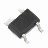
SKY65050-372LF Skyworks Solutions Inc, SKY65050-372LF Datasheet - Page 2

SKY65050-372LF
Manufacturer Part Number
SKY65050-372LF
Description
IC PHEMT 2.4GHZ 70MA LN SC70-4
Manufacturer
Skyworks Solutions Inc
Datasheet
1.SKY65050-372LF.pdf
(12 pages)
Specifications of SKY65050-372LF
Transistor Type
pHEMT FET
Frequency
2.4GHz
Gain
15.5dB
Voltage - Rated
6V
Current Rating
55mA
Noise Figure
0.4dB
Current - Test
20mA
Voltage - Test
3V
Power - Output
10.5dBm
Package / Case
SC-70-3, SOT-323-3
Lead Free Status / RoHS Status
Lead free / RoHS Compliant
Other names
863-1067-2
Available stocks
Company
Part Number
Manufacturer
Quantity
Price
Part Number:
SKY65050-372LF
Manufacturer:
SKYWORKS/思佳讯
Quantity:
20 000
DATA SHEET • SKY65050-372LF LOW NOISE TRANSISTOR
Table 1. SKY65050-372LF Signal Descriptions
Table 2. Self-Biasing Resistors
Functional Description
The SKY65050-372LF is a depletion mode pHEMT designed for
low noise, high frequency applications. The SKY65050-372LF has
a typical NF of 0.65 dB tested at the 2.4 GHz wireless LAN
frequency band. A gain of 15.5 dB typical is achieved using the
same circuit. If the frequency of operation is lowered to the 1 GHz
range, NF performance of the device can approach 0.5 dB
including input matching network losses.
De-embedded scattering and noise parameters are provided in
addition to typical circuit topologies for commonly used frequency
bands. With an appropriate circuit, the SKY65050-372LF can be
used for many applications from 450 MHz up to 6 GHz. The
compact SC-70 package makes the SKY65050-372LF an ideal
low noise and low cost solution.
Biasing
To properly bias a depletion mode pHEMT, both the gate and
drain of the device must be properly biased. At V
V
maximum amount of current, I
the best noise performance at V
control I
To eliminate the need for a negative DC supply, self-biasing
should be used when a resistor is placed between one of the
source leads and ground. A bypass capacitor should be placed in
parallel to this resistor to provide an RF ground and to ensure
performance remains unchanged at the operating frequency.
When current flows from drain to source and through the resistor,
the source voltage becomes biased above DC ground. The gate
pin of the device should be left unbiased at 0 V, which creates the
2
DS
Pin #
≥ 2 V, the device is in a saturated state and draws the
1
2
DS
, V
SOURCE
DRAIN
GS
must be biased with a negative voltage supply.
Skyworks Solutions, Inc. • Phone [781] 376-3000 • Fax [781] 376-3100 • sales@skyworksinc.com • www.skyworksinc.com
Name
November 12, 2009 • Skyworks Proprietary Information • Products and Product Information are Subject to Change Without Notice • 200967F
Resistor Value (Ω)
DSS
Source lead. Provides DC self-biasing point
and AC ground.
RF output. Requires external matching
network for optimum performance. Supply
voltage required through external RF choke.
DS
. The device typically achieves
130
47
27
20
15
10
= 3 V and I
Description
DSS
GS
= 15 mA. To
= 0 V and
Pin #
desired negative V
eliminating the need for a second DC supply.
Table 2 provides the resistor values used to properly bias the
SKY65050-372LF.
RF Matching Networks
The SKY65050-372LF Evaluation Board assembly diagram is
shown in Figure 12 and a circuit schematic is provided in
Figure 13. The schematic shows the recommended RF matching
network used for the 2.4 GHz wireless LAN frequency band. The
network was designed using de-embedded s- and n-parameters.
The circuit was primarily tuned for gain, NF, and input and output
return loss, while maintaining proper stability.
Optimal noise performance is attained when the impedance
presented to the input of the amplifier is equal to its minimum NF
impedance point. Components C1, C2, C3, L1, and L2 shown in
Figures 12 and 13 provide the necessary impedance match for NF
and input return loss. Circuit board and input matching structure
losses on the input of the amplifier directly add to the overall NF
of the amplifier. It is critical to minimize RF trace lengths and to
use high-Q components to achieve optimal NF performance.
Components R2 and C14 provide self biasing for the device and
RF grounding for one of the two source leads. Components C5
and L3 are placed on the opposing source lead and are used to
tune the transistor’s source inductance.
3
4
SOURCE
GATE
Name
GS
value. This simplifies the design by
Drain Current (mA)
Source lead. Provides DC self-biasing point
and AC ground.
RF input. Requires external matching
network for optimum performance.
10
15
20
25
30
5
Description


