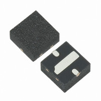
CLA4609-086LF Skyworks Solutions Inc, CLA4609-086LF Datasheet - Page 4

CLA4609-086LF
Manufacturer Part Number
CLA4609-086LF
Description
DIODE LIMITER SILICON QFN
Manufacturer
Skyworks Solutions Inc
Datasheet
1.CLA4609-086LF.pdf
(7 pages)
Specifications of CLA4609-086LF
Diode Type
PIN - Single
Voltage - Peak Reverse (max)
250V
Current - Max
200mA
Capacitance @ Vr, F
0.14pF @ 6V, 1MHz
Resistance @ If, F
1.5 Ohm @ 10mA, 500MHz
Package / Case
2-DFN
Lead Free Status / RoHS Status
Lead free / RoHS Compliant
Power Dissipation (max)
-
Other names
863-1182-2
Available stocks
Company
Part Number
Manufacturer
Quantity
Price
Company:
Part Number:
CLA4609-086LF
Manufacturer:
TOSHIBA
Quantity:
56
Part Number:
CLA4609-086LF
Manufacturer:
SKYWORKS/思佳讯
Quantity:
20 000
DATA SHEET • CLA4609-086LF SURFACE MOUNT LIMITER DIODE
Typical Performance Characteristics
(T
High Power Limiter Design Application
The CLA4609-086LF PIN limiter diode is designed for shunt
applications in receiver protection power limiter circuits.
Compared to other surface mount packages, the design of the
QFN package produces lower thermal resistance and also reduces
the effects of the parasitic inductance of the anode bond wires.
A cross-sectional view of the CLA4609-086LF PIN limiter diode is
shown in Figure 6. The cathode of the die is soldered directly to
the top of the exposed paddle. This paddle is composed of
copper, so its thermal resistance is very low.
The copper ground paddle minimizes the total thermal resistance
between the I layer, which is the location where most heat is
4
A
= 25 °C, Unless Otherwise Noted)
Figure 4. Output Power and Insertion Loss vs Input Power
+50
+45
+40
+35
+30
+25
+20
+15
+10
+10
+15
Skyworks Solutions, Inc. • Phone [781] 376-3000 • Fax [781] 376-3100 • sales@skyworksinc.com • www.skyworksinc.com
March 12, 2010 • Skyworks Proprietary Information • Products and Product Information are Subject to Change Without Notice • 201247B
Output Power
Insertion Loss
+20
Input Power (dBm)
(f = 2.0 GHz)
+25
+30
+35
Not to scale
Figure 6. Cross-Sectional View of the CLA4609-086LF
Anode
(Pin 1)
+40
Bond Wire
(2 Places)
+45
–0.15
0
–0.30
–0.45
–0.60
–0.75
–0.90
–1.05
–1.20
Cathode
(Pin 2)
generated under normal operation, and the surface to which the
package is mounted. Minimal thermal resistance between the I
layer and the external environment minimizes junction
temperature.
The electrically equivalent circuit of the CLA4609-086LF PIN
limiter diode is shown in Figure 7. The inductances of pins 1 and
2, as well as the inductances of the bond wires are in series with
the input and output transmission lines of the external circuit
rather than the portion of the circuit that contains the shunt PIN
limiter diode.
35
30
25
20
15
10
5
0
Figure 5. Typical Pulse Thermal Impedance
1
Encapsulated
Epoxy
(Pin 3)
Anode
10
Pulse Width (μs)
CLA4609-086LF Die
S1628a
100
1000


