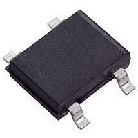
HSMS-2855-TR1G Avago Technologies US Inc., HSMS-2855-TR1G Datasheet - Page 8

HSMS-2855-TR1G
Manufacturer Part Number
HSMS-2855-TR1G
Description
DIODE SCHOTTKY DETECT SS SOT-143
Manufacturer
Avago Technologies US Inc.
Datasheet
1.HSMS-285B-BLKG.pdf
(13 pages)
Specifications of HSMS-2855-TR1G
Diode Type
Schottky - 2 Independent
Voltage - Peak Reverse (max)
2V
Capacitance @ Vr, F
0.3pF @ 1V, 1MHz
Package / Case
SOT-143, SOT-143B, TO-253AA
Diode Case Style
SOT-143
No. Of Pins
3
Peak Reflow Compatible (260 C)
Yes
Leaded Process Compatible
Yes
Forward Voltage
250mV
Repetitive Reverse Voltage Vrrm Max
2V
Pin Count
3 +Tab
Package Type
SOT-143
Forward Current If
1mA
Rohs Compliant
Yes
Lead Free Status / RoHS Status
Lead free / RoHS Compliant
Current - Max
-
Power Dissipation (max)
-
Resistance @ If, F
-
Lead Free Status / Rohs Status
Compliant
Available stocks
Company
Part Number
Manufacturer
Quantity
Price
Part Number:
HSMS-2855-TR1G
Manufacturer:
AVAGO/安华高
Quantity:
20 000
Such a circuit offers several advantages. First the voltage
outputs of two diodes are added in series, increasing the
overall value of voltage sensitivity for the network (com-
pared to a single diode detector). Second, the RF imped-
ances of the two diodes are added in parallel, making
the job of reactive matching a bit easier. Such a circuit
can easily be realized using the two series diodes in the
HSMS-285C.
Flicker Noise
Reference to Figure 5 will show that there is a junc-
tion of metal, silicon, and passivation around the rim
of the Schottky contact. It is in this three-way junction
that flicker noise
reduce the sensitivity of a crystal video receiver utiliz-
ing a Schottky detector circuit if the video frequency is
below the noise corner. Flicker noise can be substantially
reduced by the elimination of passivation, but such
diodes cannot be mounted in non-hermetic packages.
p-type silicon Schottky diodes have the least flicker noise
at a given value of external bias (compared to n-type
silicon or GaAs). At zero bias, such diodes can have
extremely low values of flicker noise. For the HSMS-285x
series, the noise temperature ratio is given in Figure 14.
Diode Burnout
Figure 14. Typical Noise Temperature Ratio.
Noise temperature ratio is the quotient of the diode’s
noise power (expressed in dBV/Hz) divided by the noise
power of an ideal resistor of resistance R = R
For an ideal resistor R, at 300°K, the noise voltage can be
computed from
which can be expressed as
Thus, for a diode with R
12.2 nV/Hz or -158 dBV/Hz. On the graph of Figure 14, -
158 dBV/Hz would replace the zero on the vertical scale
to convert the chart to one of absolute noise voltage vs.
frequency.
8
15
10
-5
5
0
10
100
FREQUENCY (Hz)
v = 1.287 X 10
[5]
1000
20 log
is generated. This noise can severely
10000
10
V
v dBV/Hz
= 9 KΩ, the noise voltage is
-10
√R volts/Hz
100000
V
.
Any Schottky junction, be it an RF diode or the gate of
a MESFET, is relatively delicate and can be burned out
with excessive RF power. Many crystal video receivers
used in RFID (tag) applications find themselves in poorly
controlled environments where high power sources may
be present. Examples are the areas around airport and
FAA radars, nearby ham radio operators, the vicinity of
a broadcast band transmitter, etc. In such environments,
the Schottky diodes of the receiver can be protected
by a device known as a limiter diode.
able only in radar warning receivers and other high cost
electronic warfare applications, these diodes have been
adapted to commercial and consumer circuits.
Avago offers a complete line of surface mountable
PIN limiter diodes. Most notably, our HSMP-4820 (SOT-
23) can act as a very fast (nanosecond) power-sensi-
tive switch when placed between the antenna and the
Schottky diode, shorting out the RF circuit temporar-
ily and reflecting the excessive RF energy back out the
antenna.
Assembly Instructions
SOT-323 PCB Footprint
A recommended PCB pad layout for the miniature SOT-
323 (SC-70) package is shown in Figure 15 (dimensions
are in inches). This layout provides ample allowance for
package placement by automated assembly equipment
without adding parasitics that could impair the perfor-
mance. Figure 16 shows the pad layout for the six-lead
SOT-363.
Figure 15. Recommended PCB
Pad Layout for Avago’s SC70
3L/SOT-323 Products.
[4]
[5]
[6]
0.039
Avago Application Note 956-4, Schottky Diode Voltage Doubler.
Avago Application Note 965-3, Flicker Noise in Schottky Diodes.
Avago Application Note 1050, Low Cost, Surface Mount Power Limiters.
0.026
Dimensions in inches
0.022
0.079
Figure 16. Recommended PCB Pad
Layout for Avago's SC70 6L/SOT-363
Products.
0.035
0.026
[6]
Formerly avail-
0.016
0.075


