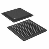
ADSP-21061LKBZ-160 Analog Devices Inc, ADSP-21061LKBZ-160 Datasheet - Page 25

ADSP-21061LKBZ-160
Manufacturer Part Number
ADSP-21061LKBZ-160
Description
DSP Floating-Point 32-Bit 40MHz 40MIPS 225-Pin BGA
Manufacturer
Analog Devices Inc
Series
SHARC®r
Type
Floating Pointr
Datasheet
1.ADSP-21061LKSZ-160.pdf
(56 pages)
Specifications of ADSP-21061LKBZ-160
Package
225BGA
Numeric And Arithmetic Format
Floating-Point
Maximum Speed
40 MHz
Ram Size
128 KB
Device Million Instructions Per Second
40 MIPS
Interface
Synchronous Serial Port (SSP)
Clock Rate
40MHz
Non-volatile Memory
External
On-chip Ram
128kB
Voltage - I/o
3.30V
Voltage - Core
3.30V
Operating Temperature
0°C ~ 85°C
Mounting Type
Surface Mount
Package / Case
225-BGA
Lead Free Status / RoHS Status
Lead free / RoHS Compliant
Available stocks
Company
Part Number
Manufacturer
Quantity
Price
Company:
Part Number:
ADSP-21061LKBZ-160
Manufacturer:
Analog Devices Inc
Quantity:
10 000
Memory Read—Bus Master
Use these specifications for asynchronous interfacing to memo-
ries (and memory-mapped peripherals) without reference to
CLKIN. These specifications apply when the ADSP-21061 is the
Table 12. Memory Read—Bus Master
1
2
3
4
Parameter
Timing Requirements
t
t
t
t
t
t
Switching Characteristics
t
t
t
t
t
W = (number of wait states specified in WAIT register)
HI = t
H = t
Data delay/setup: user must meet t
The falling edge of MSx, SW, BMS is referenced.
Data hold: user must meet t
ACK delay/setup: user must meet t
DAD
DRLD
HDA
HDRH
DAAK
DSAK
DRHA
DARL
RW
RWR
SADADC
and dc loads.
for assertion of ACK (High).
CK
CK
(if an address hold cycle occurs as specified in WAIT register; otherwise H = 0).
(if an address hold cycle or bus idle cycle occurs, as specified in WAIT register; otherwise HI = 0).
ADDRESS
MSX, SW
WR, DMAG
ADDRCLK
BMS
(OUT)
DATA
ACK
RD
Address, Selects Delay to Data Valid
RD Low to Data Valid
Data Hold from Address, Selects
Data Hold from RD High
ACK Delay from Address, Selects
ACK Delay from RD Low
Address, Selects Hold After RD High
Address, Selects to RD Low
RD Pulse Width
RD High to WR, RD, DMAGx Low
Address, Selects Setup Before ADRCLK High
HDA
or t
DAD
HDRH
DAAK
t
or t
SADADC
or synchronous spec t
or t
DRLD
DSAK
t
DARL
or synchronous spec t
t
or synchronous specification t
DAAK
1
4
3
2
t
HSDATI
DSAK
3
Figure 14. Memory Read—Bus Master
2, 4
t
DAD
Rev. C | Page 25 of 56 | July 2007
. See
1, 2
SSDATI
t
CK
Example System Hold Time Calculation on Page 44
t
DRLD
.
.
2
SACKC
(Table 13 on Page
t
RW
bus master accessing external memory space in asynchronous
access mode. Note that timing for ACK, DATA, RD, WR, and
DMAGx strobe timing parameters only applies to asynchronous
access mode.
26) for deassertion of ACK (Low), all three specifications must be met
Min
0.5
2.0
0+H
2 + 3DT/8
12.5 + 5DT/8 + W
8 + 3DT/8 + HI
0 + DT/4
ADSP-21061/ADSP-21061L
for the calculation of hold times given capacitive
5 V and 3.3 V
t
HDRH
t
t
HDA
DRHA
t
RWR
Max
18 + DT+W
12 + 5DT/8 + W
15 + 7DT/8 + W
8 + DT/2 + W
Unit
ns
ns
ns
ns
ns
ns
ns
ns
ns
ns
ns


