AD574AJDZ Analog Devices Inc, AD574AJDZ Datasheet
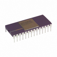
ADC Single SAR 12-Bit Parallel 28-Pin SBCDIP

AD574AJDZ

Manufacturer Part Number
AD574AJDZ
Description
ADC Single SAR 12-Bit Parallel 28-Pin SBCDIP
Manufacturer
Analog Devices Inc
Datasheets

Specifications of AD574AJDZ

Package
28SBCDIP
Resolution
12 Bit
Architecture
SAR
Number Of Adcs
1
Number Of Analog Inputs
2
Digital Interface Type
Parallel
Input Type
Voltage
Polarity Of Input Voltage
Unipolar|Bipolar
Number Of Bits
12
Sampling Rate (per Second)
28.6k
Data Interface
Parallel
Number Of Converters
1
Power Dissipation (max)
725mW
Voltage Supply Source
Dual ±
Operating Temperature
0°C ~ 70°C
Mounting Type
Through Hole
Package / Case
28-CDIP (0.600", 15.24mm)
Lead Free Status / RoHS Status
Lead free / RoHS Compliant
Lead Free Status / RoHS Status
Lead free / RoHS Compliant

Available stocks

Company
Part Number
Manufacturer
Quantity
Price
Part Number:
AD574AJDZ
Manufacturer:
AD
Quantity:
550
Part Number:
AD574AJDZ
Manufacturer:
ADI
Quantity:
478
a
PRODUCT DESCRIPTION
The AD574A is a complete 12-bit successive-approximation
analog-to-digital converter with 3-state output buffer circuitry
for direct interface to an 8- or 16-bit microprocessor bus. A high
precision voltage reference and clock are included on-chip, and
the circuit guarantees full-rated performance without external
circuitry or clock signals.
The AD574A design is implemented using Analog Devices’
Bipolar/I
tions on one chip. Offset, linearity and scaling errors are mini-
mized by active laser-trimming of thin-film resistors at the wafer
stage. The voltage reference uses an implanted buried Zener for
low noise and low drift. On the digital side, I
the successive-approximation register, control circuitry and
3-state output buffers.
The AD574A is available in six different grades. The AD574AJ,
K, and L grades are specified for operation over the 0 C to
+70 C temperature range. The AD574AS, T, and U are speci-
fied for the –55 C to +125 C range. All grades are available in a
28-pin hermetically-sealed ceramic DIP. Also, the J, K, and L
grades are available in a 28-pin plastic DIP and PLCC, and the
J and K grades are available in ceramic LCC.
The S, T, and U grades in ceramic DIP or LCC are available
with optional processing to MIL-STD-883C Class B; the T
and U grades are available as JAN QPL. The Analog Devices’
Military Products Databook should be consulted for details on
/883B testing of the AD574A.
*Protected by U.S. Patent Nos. 3,803,590; 4,213,806; 4,511,413; RE 28,633 .
REV. B
Information furnished by Analog Devices is believed to be accurate and
reliable. However, no responsibility is assumed by Analog Devices for its
use, nor for any infringements of patents or other rights of third parties
which may result from its use. No license is granted by implication or
otherwise under any patent or patent rights of Analog Devices.
FEATURES
Complete 12-Bit A/D Converter with Reference
8- and 16-Bit Microprocessor Bus Interface
Guaranteed Linearity Over Temperature
No Missing Codes Over Temperature
35 s Maximum Conversion Time
Buried Zener Reference for Long-Term Stability
Ceramic DIP, Plastic DIP or PLCC Package
Available in Higher Speed, Pinout-Compatible Versions
Available in Versions Compliant with MIL-STD-883 and
and Clock
0 C to +70 C – AD574AJ, K, L
–55 C to +125 C – AD574AS, T, U
and Low Gain T.C. 10 ppm/ C max AD574AL
(15 s AD674B, 80 s AD774B; 10 s (with SHA) AD1674)
JAN QPL
2
L process, and integrates all analog and digital func-
12.5 ppm/ C max AD574AU
2
L logic is used for
PRODUCT HIGHLIGHTS
1. The AD574A interfaces to most 8- or 16-bit microproces-
2. The precision, laser-trimmed scaling and bipolar offset resis-
3. The internal buried Zener reference is trimmed to 10.00
4. AD674B (15 s) and AD774B (8 s) provide higher speed,
One Technology Way, P.O. Box 9106, Norwood, MA 02062-9106, U.S.A.
Tel: 617/329-4700
DATA MODE SELECT
REFERENCE INPUT
sors. Multiple-mode three-state output buffers connect di-
rectly to the data bus while the read and convert commands
are taken from the control bus. The 12 bits of output data
can be read either as one 12-bit word or as two 8-bit bytes
(one with 8 data bits, the other with 4 data bits and 4 trailing
zeros).
tors provide four calibrated ranges: 0 volts to +10 volts and 0
volts to +20 volts unipolar, –5 volts to +5 volts and –10 volts
to +10 volts bipolar. Typical bipolar offset and full-scale cali-
bration errors of 0.1% can be trimmed to zero with one ex-
ternal component each.
volts with 0.2% maximum error and 15 ppm/ C typical T.C.
The reference is available externally and can drive up to
1.5 mA beyond the requirements of the reference and bipolar
offset resistors.
pin compatibility; AD1674 (10 s) includes on-chip Sample-
Hold Amplifier (SHA).
ANALOG COMMON
+10V REFERENCE
BIPOLAR OFFSET
+12/+15V SUPPLY
BYTE ADDRESS/
-12/-15V SUPPLY
10V SPAN INPUT
20V SPAN INPUT
READ/CONVERT
SHORT CYCLE
CHIP ENABLE
CHIP SELECT
+5V SUPPLY
REF OUT
BIP OFF
REF IN
V
10V
20V
LOGIC
12/8
R/C
V
V
AC
CS
CE
A
CC
EE
IN
IN
O
10
11
12
13
14
1
2
3
4
5
6
7
8
9
BLOCK DIAGRAM AND
19.95k
PIN CONFIGURATION
9.95k
10V
REF
5k
5k
12-Bit A/D Converter
CLOCK
AD574A
3k
I
REF
DAC
CONTROL
4 x N x I
I
DAC
COMP
I
12
DAC
N
=
SAR
REF
8k
V
12
EE
12
AD574A*
S
A
E
O
U
P
U
B
U
E
R
S
3
T
T
T
T
F
F
MSB
LSB
N
B
B
L
E
A
N
B
B
L
E
B
N
B
B
L
E
C
I
I
I
Complete
19
18
17
16
15
28
27
26
25
24
23
22
21
20
Fax: 617/326-8703
DB9
STATUS
STS
DB11
MSB
DB10
DB8
DB7
DB6
DB5
DB4
DB3
DB2
DB1
DB0
LSB
DIGITAL COMMON
DC
DIGITAL
DATA
OUTPUTS

Related parts for AD574AJDZ

AD574AJDZ Summary of contents

Page 1

FEATURES Complete 12-Bit A/D Converter with Reference and Clock 8- and 16-Bit Microprocessor Bus Interface Guaranteed Linearity Over Temperature +70 C – AD574AJ – +125 C – AD574AS Missing ...

Page 2

AD574A–SPECIFICATIONS Model RESOLUTION LINEARITY ERROR @ + MIN MAX DIFFERENTIAL LINEARITY ERROR (Minimum Resolution for Which No Missing Codes are Guaranteed MIN MAX UNIPOLAR OFFSET (Adjustable to Zero) BIPOLAR OFFSET (Adjustable to Zero) ...

Page 3

Model RESOLUTION LINEARITY ERROR @ + MIN MAX DIFFERENTIAL LINEARITY ERROR (Minimum Resolution for Which No Missing Codes are Guaranteed MIN MAX UNIPOLAR OFFSET (Adjustable to Zero) BIPOLAR OFFSET (Adjustable to Zero) FULL-SCALE ...

Page 4

AD574A +5V SUPPLY DATA MODE SELECT CHIP SELECT BYTE ADDRESS/ SHORT CYCLE READ/CONVERT CHIP ENABLE +12/+15V SUPPLY +10V REFERENCE ANALOG COMMON REFERENCE INPUT -12/-15V SUPPLY BIPOLAR OFFSET 10V SPAN INPUT 20V SPAN INPUT ABSOLUTE MAXIMUM RATINGS* (Specifications apply to all ...

Page 5

THE AD574A OFFERS GUARANTEED MAXIMUM LINEARITY ERROR OVER THE FULL OPERATING TEMPERATURE RANGE DEFINITIONS OF SPECIFICATIONS LINEARITY ERROR Linearity error refers to the deviation of each individual code from a line drawn from “zero” through “full scale”. The point used ...

Page 6

AD574A CIRCUIT OPERATION The AD574A is a complete 12-bit A/D converter which requires no external components to provide the complete successive- approximation analog-to-digital conversion function. A block diagram of the AD574A is shown in Figure 1. +5V SUPPLY 1 V ...

Page 7

–V REF S AGND 100 10k 10k GAIN +15V 100pF R4 100k R1 100k A1 OFFSET AD585 R3 –15V 100 ...

Page 8

AD574A The full-scale trim is done by applying a signal 1 1/2 LSB below the nominal full scale (9.9963 for range). Trim R2 to give the last transition (1111 1111 1110 to 1111 1111 1111). BIPOLAR OPERATION ...

Page 9

Figure 7 shows a complete timing diagram for the AD574A con- vert start operation. R/C should be low before both CE and CS are asserted; if R/C is high, a read operation will momentarily occur, possibly resulting in system bus ...

Page 10

AD574A to valid logic levels after the conversion cycle is completed. The STS line goes high 600 ns after R/C goes low and returns low 300 ns after data is valid. If conversion is initiated by a high pulse as ...

Page 11

Figure 15. Z80—AD574A Interface Figure 16. Wait State Generator IBM PC Interface The AD574A appears in Figure 17 interfaced to the 4 MHz 8088 processor of an IBM PC. Since the device resides in I/O space, its address is decoded ...

Page 12

AD574A 28-Pin Ceramic DIP Package (D-28) 0.048 (1.21) 0.042 (1.07) 0.458 (11.63) 0.442 (11.23) 0.075 (1.91) REF 0.075 (1.91) REF OUTLINE DIMENSIONS Dimensions shown in inches and (mm). 28-Terminal PLCC Package (P-28A) 0.180 (4.57) 0.165 (4.19) 0.048 (1.21) 0.056 (1.42) ...

Related keywords