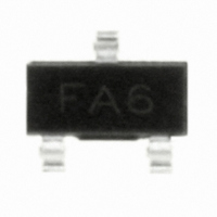
HSMP-4820-BLKG Avago Technologies US Inc., HSMP-4820-BLKG Datasheet - Page 3

HSMP-4820-BLKG
Manufacturer Part Number
HSMP-4820-BLKG
Description
DIODE PIN RF PWR LIMITER SOT-23
Manufacturer
Avago Technologies US Inc.
Datasheet
1.HSMP-3820-BLKG.pdf
(10 pages)
Specifications of HSMP-4820-BLKG
Package / Case
SOT-23-3, TO-236-3, Micro3™, SSD3, SST3
Diode Type
PIN - Single
Voltage - Peak Reverse (max)
50V
Current - Max
1A
Capacitance @ Vr, F
0.75pF @ 20V, 1MHz
Resistance @ If, F
600 mOhm @ 10mA, 1MHz
Configuration
Single Dual Anode
Reverse Voltage
50 V
Forward Continuous Current
1 A
Frequency Range
UHF or SHF
Termination Style
SMD/SMT
Maximum Diode Capacitance
1 pF @ 50 V
Maximum Operating Temperature
+ 150 C
Maximum Series Resistance @ Maximum If
0.6 Ohm @ 10 mA
Minimum Operating Temperature
- 65 C
Mounting Style
SMD/SMT
Power Dissipation
250 mW
Diode Case Style
SOT-23
Breakdown Voltage
50V
Capacitance Ct
0.8pF
Leaded Process Compatible
Yes
Peak Reflow Compatible (260 C)
Yes
Rohs Compliant
Yes
Lead Free Status / RoHS Status
Lead free / RoHS Compliant
Power Dissipation (max)
-
Lead Free Status / Rohs Status
Lead free / RoHS Compliant
Other names
516-1909
HSMP-4820-BLKG
HSMP-4820-BLKG
Available stocks
Company
Part Number
Manufacturer
Quantity
Price
Company:
Part Number:
HSMP-4820-BLKG
Manufacturer:
AVAGO
Quantity:
40 000
Part Number:
HSMP-4820-BLKG
Manufacturer:
AVAGO/安华高
Quantity:
20 000
Typical Parameters at T
Typical Applications for Multiple Diode Products
RF 1
Figure 7. Simple SPDT Switch, Using Only Positive Current.
3
Figure 1. Forward Current vs. Forward Voltage.
Figure 4. Capacitance vs. Reverse Voltage.
0.01
100
BIAS 1
1.4
1.2
1.0
0.8
0.6
0.1
10
1
0
0
V
V
0.2
F
R
10
– FORWARD VOLTAGE (mA)
– REVERSE VOLTAGE (V)
125C
0.4
20
25C
RF COMMON
0.6
–50C
30
0.8
C
= 25°C (unless otherwise noted), Single Diode
40
1.0
1.2
50
BIAS 2
Figure 5. 2nd Harmonic Input Intercept Point vs.
Forward Bias Current.
Figure 2. Reverse Recovery Time vs. Forward Current
for Various Reverse Voltages.
100
120
115
110
105
100
10
95
90
85
RF 2
1
10
1
Diode Mounted as a
Series Attenuator in a
50 Ohm Microstrip and
Tested at 123 MHz
I
F
– FORWARD BIAS CURRENT (mA)
FORWARD CURRENT (mA)
RF 1
BIAS
20
Figure 8. High Isolation SPDT Switch, Dual Bias.
10
V
V
V
R
R
R
= 10V
= 2V
= 5V
30
30
RF COMMON
Figure 6. Large Signal Transfer Curve of the
HSMP-482x Limiter.
Figure 3. RF Resistance at 25C vs. Forward Bias Current.
100
0.1
30
25
20
15
10
10
0.01
5
0
1
0
I
F
– FORWARD BIAS CURRENT (mA)
5
Measured with external
bias return
0.1
10
CW POWER IN (dBm)
15
20
1
25
1.5 GHz
30 35
10
1.0 GHz
RF 2
BIAS
100
40


