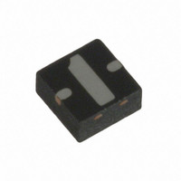
SMP1302-085LF Skyworks Solutions Inc, SMP1302-085LF Datasheet - Page 3

SMP1302-085LF
Manufacturer Part Number
SMP1302-085LF
Description
DIODE RF PIN 200V 1.5A QFN
Manufacturer
Skyworks Solutions Inc
Datasheet
1.SMP1302-085LF.pdf
(4 pages)
Specifications of SMP1302-085LF
Diode Type
PIN - Single
Voltage - Peak Reverse (max)
200V
Current - Max
1.5A
Capacitance @ Vr, F
0.35pF @ 30V, 1MHz
Resistance @ If, F
1.5 Ohm @ 100mA, 100MHz
Power Dissipation (max)
3W
Package / Case
3-VQFN
Lead Free Status / RoHS Status
Lead free / RoHS Compliant
Other names
863-1146-2
Available stocks
Company
Part Number
Manufacturer
Quantity
Price
Part Number:
SMP1302-085LF
Manufacturer:
SKYWORKS/思佳讯
Quantity:
20 000
T-R Switch Performance
1. Based on complementary pulsed bias current waveforms under RF conditions.
2. Measured with 8 µs RF pulse width, 0.5% duty cycle, 50 W ANT load.
3. F1 = 2.0155 GHz @ 10 dBm, F2 = 2.0195 GHz @ 10 dBm.
T-R Switch Circuit Diagram
Microstrip Mount
Frequency
Insertion loss (Tx-ANT)
Insertion loss (ANT-Rx)
Isolation (Rx-Tx)
Isolation (Tx-Rx)
0.1 dB Tx compression
1.0 dB Tx compression
Tx-Rx IIP3
Tx CW input power
Tx Peak input power
Rx CW input power
Tx-Rx switching speed
Tx input return loss
Rx input return loss
Thermal Via
Transmitter
(2)
Port
(1)
SMP1302-085LF
Bypass
RF
Block
DC
SMP1302-085LF
Bias 1
RF
Choke
>50 dBm (Pulsed)
46 dBm (Pulsed)
2010-2025 GHz
>49.5 dBm
>80 dBm
<0.85 µs
0.42 dB
0.45 dB
41 dBm
41 dBM
27.8 dB
28.8 dB
37.8dB
37 dB
λ/4
Block
DC
Antenna Port
High Power Switch Design Application
A T-R switch incorporating SMP1302 PIN diodes covering
2.0155 GHz to 2.0195 GHz has been designed and
tested. The switch operated safely at transmitter power
of 41dBm CW (12.6 W) with low insertion loss (0.42 dB)
and high receiver isolation (37 dB). 1 dB compression
occurred at higher than 50 dBm. In the receive state the
switch performed with 0.45 dB insertion loss and 37.8 dB
transmitter isolation.
The circuit is based on a quarter wave design utilizing two
shunt connected SMP1302 diodes. In the transmit state
the Bias 1 is set at 0 mA and Bias 2 is set at 50 mA; in the
receive state Bias 1 is set at 50 mA and Bias 2 is set at 0 mA.
Land Pattern
Block
Exposed Soldering
DC
Area Typ.
Pin 1
Part Outline
Pin 2
λ/4
Choke
RF
2X 0.25
Bias 2
2X 0.60
SMP1302-085LF
Block
Bypass
DC
RF
2X 0.55
R0.20
Receiver
Port
S1631
Pin 3
2X 0.27
2X 0.85


