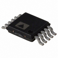
ADG736BRM Analog Devices Inc, ADG736BRM Datasheet - Page 10

ADG736BRM
Manufacturer Part Number
ADG736BRM
Description
Analog Switch Dual SPDT 10-Pin MSOP
Manufacturer
Analog Devices Inc
Type
Analog Switchr
Datasheet
1.ADG736BRMZ.pdf
(12 pages)
Specifications of ADG736BRM
Package
10MSOP
Maximum On Resistance
12@3V Ohm
Maximum High Level Output Current
30 mA
Maximum Turn-off Time
6(Typ)@3V ns
Maximum Turn-on Time
14(Typ)@3V ns
Switch Architecture
SPDT
Power Supply Type
Single
Rohs Status
RoHS non-compliant
Function
Switch
Circuit
2 x SPDT
On-state Resistance
4 Ohm
Voltage Supply Source
Single Supply
Voltage - Supply, Single/dual (±)
1.8 V ~ 5.5 V
Current - Supply
0.001µA
Operating Temperature
-40°C ~ 85°C
Mounting Type
Surface Mount
Package / Case
10-TFSOP, 10-MSOP (0.118", 3.00mm Width)
Lead Free Status / RoHS Status
Available stocks
Company
Part Number
Manufacturer
Quantity
Price
Company:
Part Number:
ADG736BRM
Manufacturer:
Wolfson
Quantity:
334
Part Number:
ADG736BRM
Manufacturer:
ADI/亚德诺
Quantity:
20 000
Company:
Part Number:
ADG736BRM-REEL
Manufacturer:
AD
Quantity:
5 510
Company:
Part Number:
ADG736BRM-REEL
Manufacturer:
NIKKO
Quantity:
5 510
Part Number:
ADG736BRM-REEL
Manufacturer:
ADI/亚德诺
Quantity:
20 000
Company:
Part Number:
ADG736BRM-REEL7
Manufacturer:
AD
Quantity:
5 510
Part Number:
ADG736BRM-REEL7
Manufacturer:
ADI/亚德诺
Quantity:
20 000
Part Number:
ADG736BRMZ
Manufacturer:
ADI/亚德诺
Quantity:
20 000
Part Number:
ADG736BRMZ-REEL
Manufacturer:
ADI/亚德诺
Quantity:
20 000
ADG736
TERMINOLOGY
R
Ohmic resistance between Terminal D and Terminal S.
ΔR
On resistance match between any two channels; that is, R
maximum − R
R
Flatness is defined as the difference between the maximum and
minimum value of on resistance as measured over the specified
analog signal range.
I
Source leakage current with the switch off.
I
Channel leakage current with the switch on.
V
Analog voltage on Terminal D and Terminal S.
C
Off switch source capacitance.
C
On switch capacitance.
t
Delay between applying the digital control input and the output
switching on. See Figure 13.
S
D
ON
ON
FLAT (ON)
S
D
D
, I
(Off)
, C
(Off)
ON
(V
S
(On)
S
S
)
(On)
ON
minimum.
ON
Rev. C | Page 10 of 12
t
Delay between applying the digital control input and the output
switching off. See Figure 13.
t
Off time or on time measured between the 90% points of both
switches, when switching from one address state to another. See
Figure 14.
Crosstalk
A measure of unwanted signal that is coupled from one channel
to another as a result of parasitic capacitance.
Off Isolation
A measure of unwanted signal coupling through an off switch.
Bandwidth
The frequency at which the output is attenuated by −3 dB.
On Response
The frequency response of the on switch.
On Loss
The voltage drop across the on switch, seen on the on response
vs. frequency plot (see Figure 7) as how many decibels (dB) the
signal is away from 0 dB at very low frequencies.
OFF
D


