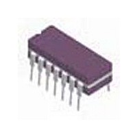
LM111J/883 National Semiconductor, LM111J/883 Datasheet - Page 11

LM111J/883
Manufacturer Part Number
LM111J/883
Description
Comparator Single ±18V/36V 14-Pin CDIP Rail
Manufacturer
National Semiconductor
Datasheet
1.LM111H883.pdf
(23 pages)
Specifications of LM111J/883
Package
14CDIP
Typical Response Time
0.2 us
Typical Response Time Range
0.05 to 0.5 us
Typical Voltage Gain Range
90 to 110 dB
Output Type
Open Collector
Number Of Channels Per Chip
1
Minimum Single Supply Voltage
5 V
Power Supply Type
Single|Dual
Number Of Elements
1
Technology
Bipolar
Input Offset Voltage
3mV
Input Bias Current (typ)
100nA
Response Time
200ns
Single Supply Voltage (typ)
9/12/15/18/24/28V
Dual Supply Voltage (typ)
±3/±5/±9/±12/±15V
Supply Current (max)
6@±15VmA
Power Supply Requirement
Single/Dual
Voltage Gain In Db
106.02dB
Single Supply Voltage (min)
5V
Single Supply Voltage (max)
36V
Dual Supply Voltage (min)
±2.5V
Dual Supply Voltage (max)
±18V
Power Dissipation
500mW
Operating Temp Range
-55C to 125C
Operating Temperature Classification
Military
Mounting
Through Hole
Pin Count
14
Package Type
CDIP
Lead Free Status / Rohs Status
Not Compliant
Available stocks
Company
Part Number
Manufacturer
Quantity
Price
Company:
Part Number:
LM111J/883B
Manufacturer:
VISHAY
Quantity:
10 931
Company:
Part Number:
LM111J/883QS
Manufacturer:
ZILOG
Quantity:
82
8.0 Application Hints
7. When both inputs of the LM111 are connected to active
Pin connections shown are for LM111H in the H08 hermetic package
Pin connections shown are for LM111H in the H08 hermetic package
signals, or if a high-impedance signal is driving the
positive input of the LM111 so that positive feedback
would be disruptive, the circuit of Figure 1 is ideal. The
positive feedback is to pin 5 (one of the offset adjust-
ment pins). It is sufficient to cause 1 to 2 mV hysteresis
and sharp transitions with input triangle waves from a
few Hz to hundreds of kHz. The positive-feedback signal
across the 82Ω resistor swings 240 mV below the posi-
(Continued)
FIGURE 2. Conventional Positive Feedback
FIGURE 1. Improved Positive Feedback
11
8. These application notes apply specifically to the LM111,
tive supply. This signal is centered around the nominal
voltage at pin 5, so this feedback does not add to the
V
trimmed out, using the 5 kΩ pot and 3 kΩ resistor as
shown.
LM211, LM311, and LF111 families of comparators, and
are applicable to all high-speed comparators in general,
(with the exception that not all comparators have trim
pins).
OS
of the comparator. As much as 8 mV of V
00570430
00570429
www.national.com
OS
can be


