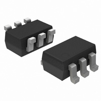
NTJS3157NT4G ON Semiconductor, NTJS3157NT4G Datasheet - Page 3

NTJS3157NT4G
Manufacturer Part Number
NTJS3157NT4G
Description
MOSFET N-CH 20V 3.2A SOT-363
Manufacturer
ON Semiconductor
Datasheet
1.NTJS3157NT1G.pdf
(6 pages)
Specifications of NTJS3157NT4G
Fet Type
MOSFET N-Channel, Metal Oxide
Fet Feature
Logic Level Gate
Rds On (max) @ Id, Vgs
60 mOhm @ 4A, 4.5V
Drain To Source Voltage (vdss)
20V
Current - Continuous Drain (id) @ 25° C
3.2A
Vgs(th) (max) @ Id
400mV @ 250µA
Gate Charge (qg) @ Vgs
15nC @ 4.5V
Input Capacitance (ciss) @ Vds
500pF @ 10V
Power - Max
1W
Mounting Type
Surface Mount
Package / Case
SC-70-6, SC-88, SOT-363
Lead Free Status / RoHS Status
Lead free / RoHS Compliant
0.25
0.15
0.05
0.2
0.1
10
8
6
4
2
0
0
0
1.8
1.6
1.4
1.2
0.8
0.6
1
−50
Figure 3. On−Resistance vs. Gate−to−Source
1
V
1
I
V
V
D
DS
Figure 1. On−Region Characteristics
GS
GS
0.8 V
= 4.0 A
−25
, DRAIN−TO−SOURCE VOLTAGE (VOLTS)
Figure 5. On−Resistance Variation with
, GATE−TO−SOURCE VOLTAGE (VOLTS)
= 4.5 V
2
8 V
4 V
2 V
T
J
3
, JUNCTION TEMPERATURE (°C)
3
0
TYPICAL PERFORMANCE CURVES
4
25
Voltage
Temperature
T
J
5
= 25°C
50
5
6
75
7
V
100
8
GS
I
T
D
J
= 4 A
= 25°C
= 1.8 V
7
1.2 V
1.6 V
1.4 V
http://onsemi.com
9
125
1 V
10
150
3
10000
1000
0.07
0.03
0.09
0.08
0.06
0.05
0.04
100
0.1
12
10
(T
2
0
8
6
4
0
2
J
1
Figure 4. On−Resistance vs. Drain Current and
= 25°C unless otherwise noted)
V
T
V
GS
J
Figure 6. Drain−to−Source Leakage Current
DS
V
= 25°C
4
V
= 0 V
DS
2
≥ 10 V
GS
0.5
, DRAIN−TO−SOURCE VOLTAGE (VOLTS)
Figure 2. Transfer Characteristics
T
, GATE−TO−SOURCE VOLTAGE (VOLTS)
J
6
= −55°C
3
I
D,
DRAIN CURRENT (AMPS)
1
8
Gate Voltage
4
T
T
V
V
V
T
vs. Voltage
J
10
J
GS
GS
GS
J
= 125°C
= 100°C
= 150°C
1.5
= 1.8 V
= 2.5 V
= 4.5 V
5
12
25°C
6
14
2
7
16
2.5
8
18
20
3
9


