NTD40N03R-1G ON Semiconductor, NTD40N03R-1G Datasheet

MOSFET N-CH 25V 7.8A IPAK

NTD40N03R-1G

Manufacturer Part Number
NTD40N03R-1G
Description
MOSFET N-CH 25V 7.8A IPAK
Manufacturer
ON Semiconductor
Datasheet

Specifications of NTD40N03R-1G

Fet Type
MOSFET N-Channel, Metal Oxide
Fet Feature
Logic Level Gate
Rds On (max) @ Id, Vgs
16.5 mOhm @ 10A, 10V
Drain To Source Voltage (vdss)
25V
Current - Continuous Drain (id) @ 25° C
7.8A
Vgs(th) (max) @ Id
2V @ 250µA
Gate Charge (qg) @ Vgs
5.78nC @ 4.5V
Input Capacitance (ciss) @ Vds
584pF @ 20V
Power - Max
1.5W
Mounting Type
Surface Mount
Package / Case
IPak, TO-251, DPak, VPak (3 straight leads + tab)
Configuration
Single
Transistor Polarity
N-Channel
Resistance Drain-source Rds (on)
0.0126 Ohms
Forward Transconductance Gfs (max / Min)
20 S
Drain-source Breakdown Voltage
25 V
Gate-source Breakdown Voltage
+/- 20 V
Continuous Drain Current
45 A
Power Dissipation
2.1 W
Maximum Operating Temperature
+ 175 C
Mounting Style
SMD/SMT
Minimum Operating Temperature
- 55 C
Lead Free Status / RoHS Status
Lead free / RoHS Compliant
Other names
NTD40N03R-1GOS

Available stocks

Company
Part Number
Manufacturer
Quantity
Price
Part Number:
NTD40N03R-1G
Manufacturer:
ON
Quantity:
12 500
NTD40N03R
Power MOSFET
45 Amps, 25 Volts
N−Channel DPAK
Features
Maximum ratings are those values beyond which device damage can occur.
Maximum ratings applied to the device are individual stress limit values (not
normal operating conditions) and are not valid simultaneously. If these limits are
exceeded, device functional operation is not implied, damage may occur and
reliability may be affected.
1. When surface mounted to an FR4 board using 0.5 sq. in pad size.
2. When surface mounted to an FR4 board using minimum recommended
© Semiconductor Components Industries, LLC, 2005
August, 2005 − Rev. 6
MAXIMUM RATINGS
Drain−to−Source Voltage
Gate−to−Source Voltage − Continuous
Thermal Resistance − Junction−to−Case
Total Power Dissipation @ T
Drain Current
Thermal Resistance − Junction−to−Ambient
(Note 1)
Thermal Resistance − Junction−to−Ambient
(Note 2)
Operating and Storage Temperature Range
Maximum Lead Temperature for Soldering
Purposes, 1/8 in from case for 10 seconds
High−Efficiency DC−DC Converters
Planar HD3e Process for Fast Switching Performance
Low R
Low C
Low Gate Charge
Optimized for High Side Switching Requirements in
Pb−Free Packages are Available
− Continuous @ T
− Continuous @ T
− Single Pulse (tp ≤ 10 ms)
pad size.
− Total Power Dissipation @ T
− Drain Current − Continuous @ T
− Total Power Dissipation @ T
− Drain Current − Continuous @ T
DS(on)
iss
to Minimize Driver Loss
to Minimize Conduction Loss
Parameter
A
C
= 25°C, Limited by Wires
= 25°C, Chip
(T
J
= 25°C unless otherwise specified)
C
= 25°C
A
A
= 25°C
= 25°C
A
A
= 25°C
= 25°C
Symbol
T
V
R
R
R
J
V
P
P
P
, T
T
DSS
I
I
I
I
I
qJC
qJA
qJA
GS
D
D
D
D
D
D
D
D
L
stg
−55 to
Value
71.4
±20
100
100
175
260
3.0
2.1
9.2
1.5
7.8
25
50
45
32
1
°C/W
°C/W
°C/W
Unit
Vdc
Vdc
°C
°C
W
W
W
A
A
A
A
A
See detailed ordering and shipping information in the package
dimensions section on page 5 of this data sheet.
Gate
(Surface Mount)
CASE 369AA
1 2
1
STYLE 2
45 AMPERES, 25 VOLTS
R
DPAK
4 Drain
Y
WW
T40N03
G
Drain
3
DS(on)
ORDERING INFORMATION
2
G
& PIN ASSIGNMENTS
MARKING DIAGRAM
http://onsemi.com
4
3
Source
N−CHANNEL
= 12.6 mW (Typ)
= Year
= Work Week
= Device Code
= Pb−Free Package
D
Publication Order Number:
Gate
S
1
(Straight Lead)
1
CASE 369D
2
STYLE 2
4 Drain
DPAK
Drain
NTD40N03R/D
3
2
4
3
Source

Related parts for NTD40N03R-1G

NTD40N03R-1G Summary of contents

Page 1

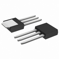
... DS(on) N−CHANNEL CASE 369D DPAK DPAK (Straight Lead) STYLE 2 MARKING DIAGRAM & PIN ASSIGNMENTS 4 Drain 4 Drain 3 2 Source 1 3 Drain Gate Source 2 Drain Y = Year WW = Work Week T40N03 = Device Code G = Pb−Free Package ORDERING INFORMATION Publication Order Number: NTD40N03R/D ...

Page 2

... SOURCE−DRAIN DIODE CHARACTERISTICS Forward On−Voltage ( Reverse Recovery Time Reverse Recovery Stored Charge 3. Pulse Test: Pulse Width ≤ 300 ms, Duty Cycle ≤ 2%. 4. Switching characteristics are independent of operating junction temperatures. NTD40N03R (T = 25°C unless otherwise specified) J V(br) = 150° Vdc MHz) ...

Page 3

... DRAIN CURRENT (AMPS) D Figure 3. On−Resistance versus Drain Current and Temperature 1 1.6 GS 1.4 1.2 1 0.8 0.6 −50 − JUNCTION TEMPERATURE (°C) J Figure 5. On−Resistance Variation with Temperature NTD40N03R 20 ≥ GATE−TO−SOURCE VOLTAGE (VOLTS) GS Figure 2. Transfer Characteristics 0.040 0.032 0.024 ...

Page 4

... Figure 7. Capacitance Variation 100 d(off d(on GATE RESISTANCE (W) G Figure 9. Resistive Switching Time Variation versus Gate Resistance 100 SINGLE PULSE 0.1 Figure 11. Maximum Rated Forward Biased NTD40N03R 25° iss oss 2 C rss Drain−to−Source Voltage versus Total Charge 25° 100 ...

Page 5

... SINGLE PULSE 0.01 0.00001 0.0001 ORDERING INFORMATION Device NTD40N03R NTD40N03RG NTD40N03R−1 NTD40N03R−1G NTD40N03RT4 NTD40N03RT4G †For information on tape and reel specifications, including part orientation and tape sizes, please refer to our Tape and Reel Packaging Specifications Brochure, BRD8011/D. NTD40N03R P (pk DUTY CYCLE ...

Page 6

... 0.13 (0.005) M 5.80 0.228 *For additional information on our Pb−Free strategy and soldering details, please download the ON Semiconductor Soldering and Mounting Techniques Reference Manual, SOLDERRM/D. NTD40N03R PACKAGE DIMENSIONS DPAK (SINGLE GAUGE) CASE 369AA−01 ISSUE O SEATING −T− PLANE SOLDERING FOOTPRINT* 6.20 3 ...

Page 7

... S 0.025 0.040 0.63 1.01 V 0.035 0.050 0.89 1.27 Z 0.155 −−− 3.93 −−− STYLE 2: PIN 1. GATE 2. DRAIN 3. SOURCE 4. DRAIN ON Semiconductor Website: http://onsemi.com Order Literature: http://www.onsemi.com/litorder For additional information, please contact your local Sales Representative. NTD40N03R/D ...

Related keywords