NTD3055L170-001 ON Semiconductor, NTD3055L170-001 Datasheet - Page 7
NTD3055L170-001
Manufacturer Part Number
NTD3055L170-001
Description
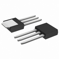
MOSFET N-CH 60V 9A TO-251A
Manufacturer
ON Semiconductor
Datasheet
1.NTD3055L170T4G.pdf
(8 pages)
Specifications of NTD3055L170-001
Fet Type
MOSFET N-Channel, Metal Oxide
Fet Feature
Logic Level Gate
Rds On (max) @ Id, Vgs
170 mOhm @ 4.5A, 5V
Drain To Source Voltage (vdss)
60V
Current - Continuous Drain (id) @ 25° C
9A
Vgs(th) (max) @ Id
2V @ 250µA
Gate Charge (qg) @ Vgs
10nC @ 5V
Input Capacitance (ciss) @ Vds
275pF @ 25V
Power - Max
1.5W
Mounting Type
Surface Mount
Package / Case
IPak, TO-251, DPak, VPak (3 straight leads + tab)
Lead Free Status / RoHS Status
Contains lead / RoHS non-compliant
Other names
NTD3055L170-001OS


V
S
F
1
B
R
G
4
2
3
L
A
K
D
2 PL
0.13 (0.005)
*For additional information on our Pb−Free strategy and soldering
details, please download the ON Semiconductor Soldering and
Mounting Techniques Reference Manual, SOLDERRM/D.
H
0.228
J
5.80
M
C
T
−T−
PACKAGE DIMENSIONS
SOLDERING FOOTPRINT*
E
0.244
6.20
SEATING
PLANE
U
http://onsemi.com
CASE 369C−01
ISSUE C
DPAK
0.101
2.58
7
0.118
3.0
0.063
1.6
SCALE 3:1
6.172
0.243
Z
inches
mm
NOTES:
1. DIMENSIONING AND TOLERANCING
2. CONTROLLING DIMENSION: INCH.
PER ANSI Y14.5M, 1982.
STYLE 2:
DIM
G
A
B
C
D
E
F
H
K
L
R
S
U
V
Z
PIN 1. GATE
J
2. DRAIN
3. SOURCE
4. DRAIN
0.235
0.250
0.086
0.027
0.018
0.037
0.034
0.018
0.102
0.180
0.025
0.020
0.035
0.155
MIN
0.180 BSC
0.090 BSC
INCHES
0.245
0.265
0.094
0.035
0.023
0.045
0.040
0.023
0.114
0.215
0.040
0.050
MAX
−−−
−−−
MILLIMETERS
5.97
6.35
2.19
0.69
0.46
0.94
0.87
0.46
2.60
4.57
0.63
0.51
0.89
3.93
MIN
4.58 BSC
2.29 BSC
MAX
6.22
6.73
2.38
0.88
0.58
1.14
1.01
0.58
2.89
5.45
1.01
1.27
−−−
−−−
Related parts for NTD3055L170-001
Image
Part Number
Description
Manufacturer
Datasheet
Request
R

Part Number:
Description:
ON Semiconductor [VOLTAGE REGULATOR]
Manufacturer:
ON Semiconductor
Datasheet:
Part Number:
Description:
357-036-542-201 CARDEDGE 36POS DL .156 BLK LOPRO
Manufacturer:
ON Semiconductor
Datasheet:
Part Number:
Description:
357-036-542-201 CARDEDGE 36POS DL .156 BLK LOPRO
Manufacturer:
ON Semiconductor
Datasheet:
Part Number:
Description:
357-036-542-201 CARDEDGE 36POS DL .156 BLK LOPRO
Manufacturer:
ON Semiconductor
Datasheet:
Part Number:
Description:
357-036-542-201 CARDEDGE 36POS DL .156 BLK LOPRO
Manufacturer:
ON Semiconductor
Datasheet:
Part Number:
Description:
357-036-542-201 CARDEDGE 36POS DL .156 BLK LOPRO
Manufacturer:
ON Semiconductor
Datasheet:
Part Number:
Description:
357-036-542-201 CARDEDGE 36POS DL .156 BLK LOPRO
Manufacturer:
ON Semiconductor
Datasheet:
Part Number:
Description:
357-036-542-201 CARDEDGE 36POS DL .156 BLK LOPRO
Manufacturer:
ON Semiconductor
Datasheet:
Part Number:
Description:
357-036-542-201 CARDEDGE 36POS DL .156 BLK LOPRO
Manufacturer:
ON Semiconductor
Datasheet:
Part Number:
Description:
357-036-542-201 CARDEDGE 36POS DL .156 BLK LOPRO
Manufacturer:
ON Semiconductor
Datasheet:
Part Number:
Description:
357-036-542-201 CARDEDGE 36POS DL .156 BLK LOPRO
Manufacturer:
ON Semiconductor
Datasheet:
Part Number:
Description:
Manufacturer:
ON Semiconductor
Datasheet:
Part Number:
Description:
Manufacturer:
ON Semiconductor
Datasheet: