IRFBA22N50A Vishay, IRFBA22N50A Datasheet
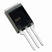
MOSFET N-CH 500V 24A SUPER-220

IRFBA22N50A

Manufacturer Part Number
IRFBA22N50A
Description
MOSFET N-CH 500V 24A SUPER-220
Manufacturer
Vishay
Series
HEXFET®r
Datasheet

Specifications of IRFBA22N50A

Fet Type
MOSFET N-Channel, Metal Oxide
Fet Feature
Standard
Rds On (max) @ Id, Vgs
230 mOhm @ 13.8A, 10V
Drain To Source Voltage (vdss)
500V
Current - Continuous Drain (id) @ 25° C
24A
Vgs(th) (max) @ Id
4V @ 250µA
Gate Charge (qg) @ Vgs
115nC @ 10V
Input Capacitance (ciss) @ Vds
3400pF @ 25V
Power - Max
340W
Mounting Type
Through Hole
Package / Case
Super-220™
Lead Free Status / RoHS Status
Contains lead / RoHS non-compliant

Available stocks

Company
Part Number
Manufacturer
Quantity
Price
Part Number:
IRFBA22N50A
Manufacturer:
VISHAY
Quantity:
5 000
l
l
l
l
l
l
l
l
l
I
I
I
P
V
T
T
dv/dt
Notes  through …
D
D
DM
www.irf.com
J
STG
D
GS
@ T
@ T
@T
Drive Requirement
dv/dt Ruggedness
Avalanche Voltage and Current
Switch Mode Power Supply ( SMPS )
Uninterruptible Power Supply
High Speed Power Switching
Low Gate Charge Qg results in Simple
Improved Gate, Avalanche and Dynamic
Fully Characterized Capacitance and
Effective Coss Specified (See AN1001)
Full Bridge Converters
Power Factor Correction Boost
C
C
C
= 25°C
= 100°C
= 25°C
Continuous Drain Current, V
Pulsed Drain Current 
Power Dissipation
Linear Derating Factor
Gate-to-Source Voltage
Peak Diode Recovery dv/dt ƒ
Operating Junction and
Storage Temperature Range
Soldering Temperature, for 10 seconds
Recommended clip force
are on page 8
Parameter
SMPS MOSFET
GS
GS
@ 10V
@ 10V
V
500V
DSS
300 (1.6mm from case )
HEXFET Power MOSFET
-55 to + 150
R
Max.
340
± 30
20
2.7
3.4
24
15
96
DS(on)
0.23
max
Units
W/°C
V/ns
24A
°C
W
N
A
V
I
D
1
8/15/02

Related parts for IRFBA22N50A

IRFBA22N50A Summary of contents

Page 1

Switch Mode Power Supply ( SMPS ) l Uninterruptible Power Supply l l High Speed Power Switching l Low Gate Charge Qg results in Simple Drive Requirement l Improved Gate, Avalanche and Dynamic dv/dt Ruggedness Fully Characterized Capacitance and l ...

Page 2

Static @ T = 25°C (unless otherwise specified) J Parameter V Drain-to-Source Breakdown Voltage (BR)DSS R Static Drain-to-Source On-Resistance DS(on) V Gate Threshold Voltage GS(th) I Drain-to-Source Leakage Current DSS Gate-to-Source Forward Leakage I GSS Gate-to-Source Reverse Leakage Dynamic @ ...

Page 3

VGS TOP 15V 10V 8.0V 7.0V 6.0V 5.5V 5.0V BOTTOM 4. 4.5V 20µs PULSE WIDTH 0.1 0 Drain-to-Source Voltage (V) DS Fig 1. Typical Output Characteristics 100 T = ...

Page 4

1MHz iss 6000 rss oss ds gd 5000 4000 C iss 3000 C oss 2000 ...

Page 5

T , Case Temperature ( C) C Fig 9. Maximum Drain Current Vs. Case Temperature 0.50 0.1 0.20 0.10 0.05 0.02 0.01 0.01 SINGLE PULSE (THERMAL RESPONSE) ...

Page 6

D.U 20V 0. Fig 12a. Unclamped Inductive Test Circuit V (BR)DSS Fig 12b. Unclamped Inductive Waveforms Charge Fig 13a. ...

Page 7

D.U.T + ‚ -  Driver Gate Drive P.W. D.U.T. I Waveform SD Reverse Recovery Current D.U.T. V Waveform DS Re-Applied Voltage Inductor Curent Fig 14. For N-Channel HEXFET www.irf.com + ƒ - „ P.W. Period D = ...

Page 8

A 1.50 [.059] 0.50 [.020 4.00 [.157] 3.50 [.138] 3X 2.55 [.100] 0.25 [.010] 2X Notes:  Repetitive rating; pulse width limited by max. junction temperature. ( See fig ‚ Starting T = 25°C, L ...

Related keywords