IRF730AS Vishay, IRF730AS Datasheet
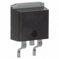
MOSFET N-CH 400V 5.5A D2PAK

IRF730AS

Manufacturer Part Number
IRF730AS
Description
MOSFET N-CH 400V 5.5A D2PAK
Manufacturer
Vishay
Datasheet

Specifications of IRF730AS

Fet Type
MOSFET N-Channel, Metal Oxide
Fet Feature
Standard
Rds On (max) @ Id, Vgs
1 Ohm @ 3.3A, 10V
Drain To Source Voltage (vdss)
400V
Current - Continuous Drain (id) @ 25° C
5.5A
Vgs(th) (max) @ Id
4.5V @ 250µA
Gate Charge (qg) @ Vgs
22nC @ 10V
Input Capacitance (ciss) @ Vds
600pF @ 25V
Power - Max
74W
Mounting Type
Surface Mount
Package / Case
D²Pak, TO-263 (2 leads + tab)
Lead Free Status / RoHS Status
Contains lead / RoHS non-compliant
Other names
*IRF730AS

Available stocks

Company
Part Number
Manufacturer
Quantity
Price
Part Number:
IRF730AS
Manufacturer:
IR
Quantity:
12 500
Company:
Part Number:
IRF730ASPBF
Quantity:
230
Company:
Part Number:
IRF730ASTRLPBF
Quantity:
1 165
Part Number:
IRF730ASTRPBF
Manufacturer:
IR
Quantity:
20 000
Part Number:
IRF730ASTRRPBF
Manufacturer:
IR
Quantity:
23 000
Note
a. See device orientation.
Notes
a. Repetitive rating; pulse width limited by maximum junction temperature (see fig. 11).
b. Starting T
c. I
d. 1.6 mm from case.
e. Uses IRF730A, SiHF730A data and test conditions.
* Pb containing terminations are not RoHS compliant, exemptions may apply
Document Number: 91046
S-83000-Rev. A, 19-Jan-09
I
2
PAK
PRODUCT SUMMARY
V
R
Q
Q
Q
Configuration
ORDERING INFORMATION
Package
Lead (Pb)-free
SnPb
ABSOLUTE MAXIMUM RATINGS T
PARAMETER
Drain-Source Voltage
Gate-Source Voltage
Continuous Drain Current
Pulsed Drain Current
Linear Derating Factor
Single Pulse Avalanche Energy
Avalanche Current
Repetiitive Avalanche Energy
Maximum Power Dissipation
Peak Diode Recovery dV/dt
Operating Junction and Storage Temperature Range
Soldering Recommendations (Peak Temperature)
DS
DS(on)
g
gs
gd
SD
(Max.) (nC)
(nC)
(nC)
(V)
≤ 5.5 A, dI/dt ≤ 90 A/µs, V
(TO-262)
(Max.) (Ω)
J
= 25 °C, L = 19 mH, R
G
D
S
a
G
D
a, e
D
2
PAK (TO-263)
S
c, e
D
IRF730ASPbF
SiHF730AS-E3
IRF730AS
SiHF730AS
a
2
DD
PAK (TO-263)
b, e
V
≤ V
GS
G
= 25 Ω, I
= 10 V
DS
, T
G
J
IRF730AS, SiHF730AS, IRF730AL, SiHF730AL
Single
≤ 150 °C.
N-Channel MOSFET
400
5.8
9.3
22
AS
= 5.5 A (see fig. 12).
C
Power MOSFET
D
S
= 25 °C, unless otherwise noted
V
1.0
GS
D
IRF730ASTRLPbF
SiHF730ASTL-E3
IRF730ASTRL
SiHF730ASTL
at 10 V
2
PAK (TO-263)
T
for 10 s
C
= 25 °C
T
T
C
C
a
a
= 100 °C
= 25 °C
FEATURES
• Low Gate Charge Q
• Improved Gate, Avalanche and Dynamic dV/dt
• Fully Characterized Capacitance and Avalanche Voltage
• Effective C
• Lead (Pb)-free Available
APPLICATIONS
• Switch Mode Power Supply (SMPS)
• Uninterruptible Power Supply
• High Sspeed Power Switching
TYPICAL SMPS TOPOLOGIES
• Single Transistor Flyback Xfmr. Reset
• Single Transistor Forward Xfmr. Reset (Both US Line Input
a
Requirement
Ruggedness
and Current
Only)
a
SYMBOL
D
IRF730ASTRRPbF
SiHF730ASTR-E3
-
-
T
2
dV/dt
oss
J
PAK (TO-263)
V
V
E
E
I
I
P
, T
I
DM
AR
DS
GS
AS
AR
D
D
stg
Specified
g
Results in Simple Drive
a
a
- 55 to + 150
LIMIT
300
± 30
400
290
5.5
3.5
0.6
5.5
7.4
4.6
22
74
Vishay Siliconix
d
I
IRF730ALPbF
SiHF730AL-E3
-
-
2
PAK (TO-262)
www.vishay.com
UNIT
W/°C
V/ns
RoHS*
COMPLIANT
mJ
mJ
°C
W
V
A
A
Available
1

Related parts for IRF730AS

IRF730AS Summary of contents

Page 1

... 1.6 mm from case. e. Uses IRF730A, SiHF730A data and test conditions containing terminations are not RoHS compliant, exemptions may apply Document Number: 91046 S-83000-Rev. A, 19-Jan-09 IRF730AS, SiHF730AS, IRF730AL, SiHF730AL Power MOSFET FEATURES • Low Gate Charge Q 400 Requirement 1.0 • Improved Gate, Avalanche and Dynamic dV/dt ...

Page 2

... IRF730AS, SiHF730AS, IRF730AL, SiHF730AL Vishay Siliconix THERMAL RESISTANCE RATINGS PARAMETER Maximum Junction-to-Ambient a (PCB Mounted, steady-state) Maximum Junction-to-Case (Drain) Note a. When mounted on 1" square PCB (FR-4 or G-10 material). SPECIFICATIONS °C, unless otherwise noted J PARAMETER Static Drain-Source Breakdown Voltage V Temperature Coefficient DS Gate-Source Threshold Voltage ...

Page 3

... V 8 7.0 V 6.0 V 5 Bottom 4 Drain-to-Source Voltage ( 91046_02 Fig Typical Output Characteristics Document Number: 91046 S-83000-Rev. A, 19-Jan-09 IRF730AS, SiHF730AS, IRF730AL, SiHF730AL 4 µs Pulse Width ° 91046_03 4 µs Pulse Width T = 150 ° 91046_04 Fig Normalized On-Resistance vs. Temperature Vishay Siliconix ...

Page 4

... IRF730AS, SiHF730AS, IRF730AL, SiHF730AL Vishay Siliconix MHz iss rss oss Drain-to-Source Voltage ( 91046_05 Fig Typical Capacitance vs. Drain-to-Source Voltage 5 320 200 Total Gate Charge (nC) 91046_06 G Fig Typical Gate Charge vs. Gate-to-Source Voltage www.vishay.com Shorted iss C oss C rss 0 91046_07 Fig Typical Source-Drain Diode Forward Voltage ...

Page 5

... Fig Maximum Effective Transient Thermal Impedance, Junction-to-Case D.U 0.01 Ω Fig. 12a - Unclamped Inductive Test Circuit Document Number: 91046 S-83000-Rev. A, 19-Jan-09 IRF730AS, SiHF730AS, IRF730AL, SiHF730AL 125 150 Single Pulse (Thermal Response Rectangular Pulse Duration ( Driver + - Vishay Siliconix ...

Page 6

... IRF730AS, SiHF730AS, IRF730AL, SiHF730AL Vishay Siliconix 700 600 500 400 300 200 100 100 Starting T , Junction Temperature (°C) 91046_12c J Fig. 12c - Maximum Avalanche Energy vs. Drain Current Charge Fig. 13a - Maximum Avalanche Energy vs. Drain Current www.vishay.com 6 610 600 I 590 D Top 2.5 A 3.5 A ...

Page 7

... Technology and Package Reliability represent a composite of all qualified locations. For related documents such as package/tape drawings, part marking, and reliability data, see www.vishay.com/ppg?91046. Document Number: 91046 S-83000-Rev. A, 19-Jan-09 IRF730AS, SiHF730AS, IRF730AL, SiHF730AL Peak Diode Recovery dV/dt Test Circuit + Circuit layout considerations • Low stray inductance • ...

Page 8

... Vishay disclaims any and all liability arising out of the use or application of any product described herein or of any information provided herein to the maximum extent permitted by law. The product specifications do not expand or otherwise modify Vishay’ ...

Related keywords