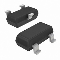
NTR1P02LT1G ON Semiconductor, NTR1P02LT1G Datasheet

MOSFET P-CH 20V 1.3A SOT-23

NTR1P02LT1G

Manufacturer Part Number
NTR1P02LT1G
Description
MOSFET P-CH 20V 1.3A SOT-23
Manufacturer
ON Semiconductor
Type
Power MOSFETr
Datasheet

Specifications of NTR1P02LT1G

Fet Type
MOSFET P-Channel, Metal Oxide
Fet Feature
Logic Level Gate
Rds On (max) @ Id, Vgs
220 mOhm @ 750mA, 4.5V
Drain To Source Voltage (vdss)
20V
Current - Continuous Drain (id) @ 25° C
1.3A
Vgs(th) (max) @ Id
1.25V @ 250µA
Gate Charge (qg) @ Vgs
5.5nC @ 4V
Input Capacitance (ciss) @ Vds
225pF @ 5V
Power - Max
400mW
Mounting Type
Surface Mount
Package / Case
SOT-23-3, TO-236-3, Micro3™, SSD3, SST3
Transistor Polarity
P Channel
Continuous Drain Current Id
1.3mA
Drain Source Voltage Vds
-20V
On Resistance Rds(on)
220mohm
Rds(on) Test Voltage Vgs
-4.5V
Threshold Voltage Vgs Typ
-1V
Rohs Compliant
Yes
Number Of Elements
1
Polarity
P
Channel Mode
Enhancement
Drain-source On-res
0.22Ohm
Drain-source On-volt
20V
Gate-source Voltage (max)
±12V
Drain Current (max)
1.3A
Power Dissipation
400mW
Output Power (max)
Not RequiredW
Frequency (max)
Not RequiredMHz
Noise Figure
Not RequireddB
Power Gain
Not RequireddB
Drain Efficiency
Not Required%
Operating Temp Range
-55C to 150C
Operating Temperature Classification
Military
Mounting
Surface Mount
Pin Count
3
Package Type
SOT-23
Configuration
Single
Resistance Drain-source Rds (on)
0.22 Ohm @ 4.5 V
Drain-source Breakdown Voltage
20 V
Gate-source Breakdown Voltage
+/- 12 V
Continuous Drain Current
1.3 A
Maximum Operating Temperature
+ 150 C
Mounting Style
SMD/SMT
Minimum Operating Temperature
- 55 C
Lead Free Status / RoHS Status
Lead free / RoHS Compliant
Other names
NTR1P02LT1GOSTR

Available stocks

Company
Part Number
Manufacturer
Quantity
Price
Part Number:
NTR1P02LT1G
Manufacturer:
ON
Quantity:
9 000
Part Number:
NTR1P02LT1G
Manufacturer:
ON
Quantity:
2 503
Part Number:
NTR1P02LT1G
Manufacturer:
ON
Quantity:
30 000
Part Number:
NTR1P02LT1G
Manufacturer:
ON/安森美
Quantity:
20 000
Part Number:
NTR1P02LT1G
0
Company:
Part Number:
NTR1P02LT1G
Quantity:
117 000
Company:
Part Number:
NTR1P02LT1G
Quantity:
25 760
Company:
Part Number:
NTR1P02LT1G
Quantity:
1 760
NTR1P02LT1
Power MOSFET
−20 V, −1.3 A, P−Channel
SOT−23 Package
minimal power loss and conserve energy, making these devices ideal
for use in space sensitive power management circuitry. Typical
applications are DC−DC converters and power management in
portable and battery−powered products such as computers, printers,
PCMCIA cards, cellular and cordless telephones.
Features
Stresses exceeding Maximum Ratings may damage the device. Maximum
Ratings are stress ratings only. Functional operation above the Recommended
Operating Conditions is not implied. Extended exposure to stresses above the
Recommended Operating Conditions may affect device reliability.
© Semiconductor Components Industries, LLC, 2006
May, 2006 − Rev. 8
MAXIMUM RATINGS
Drain−to−Source Voltage
Gate−to−Source Voltage − Continuous
Total Power Dissipation @ T
Operating and Storage Temperature Range
Thermal Resistance − Junction−to−Ambient
Maximum Lead Temperature for Soldering
Drain Current
These miniature surface mount MOSFETs low R
Low R
Miniature SOT−23 Surface Mount Package Saves Board Space
Pb−Free Packages are Available
Purposes, (1/8″ from case for 10 s)
− Continuous @ T
− Pulsed Drain Current (t
DS(on)
Provides Higher Efficiency and Extends Battery Life
Rating
A
= 25°C
(T
J
= 25°C unless otherwise noted)
A
p
= 25°C
≤ 10 ms)
Symbol
T
V
R
V
J
I
P
, T
T
DSS
DM
I
qJA
GS
D
D
L
stg
− 55 to
Value
DS(on)
−1.3
−4.0
−20
±12
400
150
300
260
1
assure
°C/W
Unit
mW
°C
°C
V
V
A
A
NTR1P02LT1G
NTR1P02LT3G
†For information on tape and reel specifications,
NTR1P02LT1
NTR1P02LT3
including part orientation and tape sizes, please
refer to our Tape and Reel Packaging Specifications
Brochure, BRD8011/D.
V
1
CASE 318
(BR)DSS
−20 V
STYLE 21
(Note: Microdot may be in either location)
*Date Code orientation may vary depending
Device
SOT−23
upon manufacturing location.
2
P02
M
G
ORDERING INFORMATION
G
http://onsemi.com
3
(Pb−Free)
(Pb−Free)
= Specific Device Code
= Date Code*
= Pb−Free Package
Package
SOT−23
SOT−23
SOT−23
SOT−23
R
DS(on)
220 mW
MARKING DIAGRAM &
P−Channel
PIN ASSIGNMENT
Publication Order Number:
Gate
D
S
Max
1
10,000 Tape & Reel
10,000 Tape & Reel
P02 M G
3000 Tape & Reel
3000 Tape & Reel
Drain
3
G
Shipping
NTR1P02LT1/D
Source
2
I
−1.3 A
D
Max

Related parts for NTR1P02LT1G

NTR1P02LT1G Summary of contents

Page 1

... L (Note: Microdot may be in either location) *Date Code orientation may vary depending upon manufacturing location. Device NTR1P02LT1 NTR1P02LT1G NTR1P02LT3 NTR1P02LT3G †For information on tape and reel specifications, including part orientation and tape sizes, please refer to our Tape and Reel Packaging Specifications Brochure, BRD8011/D. ...

Page 2

ELECTRICAL CHARACTERISTICS Characteristic OFF CHARACTERISTICS Drain−to−Source Breakdown Voltage ( −10 mA Zero Gate Voltage Drain Current (V = − − ...

Page 3

V = − −2 V −2 −2.6 V −2.4 V 1.5 −2 0.5 −1 −V , DRAIN−TO−SOURCE VOLTAGE (VOLTS) DS Figure 1. On−Region Characteristics 0. ...

Page 4

4500 DS 4000 3500 3000 2500 2000 1500 1000 500 −V − GATE−TO−SOURCE OR DRAIN−TO−SOURCE VOLTAGE (VOLTS) Figure 7. Capacitance Variation 100 V = − ...

Page 5

... A A1 *For additional information on our Pb−Free strategy and soldering details, please download the ON Semiconductor Soldering and Mounting Techniques Reference Manual, SOLDERRM/D. ON Semiconductor and are registered trademarks of Semiconductor Components Industries, LLC (SCILLC). SCILLC reserves the right to make changes without further notice to any products herein. SCILLC makes no warranty, representation or guarantee regarding the suitability of its products for any particular purpose, nor does SCILLC assume any liability arising out of the application or use of any product or circuit, and specifically disclaims any and all liability, including without limitation special, consequential or incidental damages. “ ...

Related keywords