NTD12N10T4G ON Semiconductor, NTD12N10T4G Datasheet
NTD12N10T4G
Specifications of NTD12N10T4G
NTD12N10T4GOS
NTD12N10T4GOSTR
Available stocks


Related parts for NTD12N10T4G

NTD12N10T4G Summary of contents
Page 1
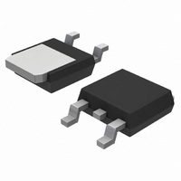
NTD12N10 Power MOSFET 12 Amps, 100 Volts N−Channel Enhancement−Mode DPAK Features • Source−to−Drain Diode Recovery Time Comparable to a Discrete Fast Recovery Diode • Avalanche Energy Specified • I and R Specified at Elevated Temperature DSS DS(on) • Mounting Information ...
Page 2
... Indicates Pulse Test: P.W. = 300 ms max, Duty Cycle = 2%. 5. Switching characteristics are independent of operating junction temperature. ORDERING INFORMATION Device NTD12N10G NTD12N10−1G NTD12N10T4G †For information on tape and reel specifications, including part orientation and tape sizes, please refer to our Tape and Reel Packaging Specifications Brochure, BRD8011/ 25°C unless otherwise noted) C ...
Page 3
TYPICAL ELECTRICAL CHARACTERISTICS 7 DRAIN−TO−SOURCE VOLTAGE (VOLTS) DS Figure 1. On−Region Characteristics ...
Page 4
Switching behavior is most easily modeled and predicted by recognizing that the power MOSFET is charge controlled. The lengths of various switching intervals (Dt) are determined by how fast the FET input capacitance can be charged by current from the ...
Page 5
TOTAL GATE CHARGE (nC) G Figure 8. Gate−To−Source and Drain−To−Source Voltage versus Total Charge ...
Page 6
SINGLE PULSE T = 25° 100 LIMIT DS(on) THERMAL LIMIT PACKAGE LIMIT 0.1 0 DRAIN−TO−SOURCE VOLTAGE (VOLTS) DS Figure 11. Maximum Rated Forward Biased Safe Operating ...
Page 7
... 0.13 (0.005) M 5.80 0.228 *For additional information on our Pb−Free strategy and soldering details, please download the ON Semiconductor Soldering and Mounting Techniques Reference Manual, SOLDERRM/D. PACKAGE DIMENSIONS DPAK (SINGLE GAUGE) CASE 369C−01 ISSUE C SEATING −T− PLANE RECOMMENDED FOOTPRINT* 6.20 3.0 ...
Page 8
... Opportunity/Affirmative Action Employer. This literature is subject to all applicable copyright laws and is not for resale in any manner. PUBLICATION ORDERING INFORMATION LITERATURE FULFILLMENT: Literature Distribution Center for ON Semiconductor P.O. Box 5163, Denver, Colorado 80217 USA Phone: 303−675−2175 or 800−344−3860 Toll Free USA/Canada Fax: 303− ...