NTR0202PLT1G ON Semiconductor, NTR0202PLT1G Datasheet - Page 2
NTR0202PLT1G
Manufacturer Part Number
NTR0202PLT1G
Description
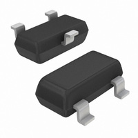
MOSFET P-CH 20V 400MA SOT-23
Manufacturer
ON Semiconductor
Type
Power MOSFETr
Datasheet
1.NTR0202PLT1G.pdf
(5 pages)
Specifications of NTR0202PLT1G
Fet Type
MOSFET P-Channel, Metal Oxide
Fet Feature
Logic Level Gate
Rds On (max) @ Id, Vgs
800 mOhm @ 200mA, 10V
Drain To Source Voltage (vdss)
20V
Current - Continuous Drain (id) @ 25° C
400mA
Vgs(th) (max) @ Id
2.3V @ 250µA
Gate Charge (qg) @ Vgs
2.18nC @ 10V
Input Capacitance (ciss) @ Vds
70pF @ 5V
Power - Max
225mW
Mounting Type
Surface Mount
Package / Case
SOT-23-3, TO-236-3, Micro3™, SSD3, SST3
Configuration
Single
Transistor Polarity
P-Channel
Resistance Drain-source Rds (on)
0.8 Ohm @ 10 V
Forward Transconductance Gfs (max / Min)
0.5 S
Drain-source Breakdown Voltage
20 V
Gate-source Breakdown Voltage
+/- 20 V
Continuous Drain Current
0.4 A
Power Dissipation
225 mW
Maximum Operating Temperature
+ 150 C
Mounting Style
SMD/SMT
Minimum Operating Temperature
- 55 C
Number Of Elements
1
Polarity
P
Channel Mode
Enhancement
Drain-source On-res
0.8Ohm
Drain-source On-volt
20V
Gate-source Voltage (max)
±20V
Drain Current (max)
400mA
Output Power (max)
Not RequiredW
Frequency (max)
Not RequiredMHz
Noise Figure
Not RequireddB
Power Gain
Not RequireddB
Drain Efficiency
Not Required%
Operating Temp Range
-55C to 150C
Operating Temperature Classification
Military
Mounting
Surface Mount
Pin Count
3
Package Type
SOT-23
Lead Free Status / RoHS Status
Lead free / RoHS Compliant
Other names
NTR0202PLT1GOSTR
Available stocks
Company
Part Number
Manufacturer
Quantity
Price
Company:

Part Number:
NTR0202PLT1G
Manufacturer:
ON
Quantity:
9 000
Company:
Part Number:
NTR0202PLT1G
Manufacturer:
ON Semiconductor
Quantity:
12 550
Company:
Part Number:
NTR0202PLT1G
Manufacturer:
ON
Quantity:
30 000
Part Number:
NTR0202PLT1G
Manufacturer:
ON/安森美
Quantity:
20 000


2. Pulse Test: Pulse Width ≤ 300 ms, Duty Cycle ≤ 2%.
3. Switching characteristics are independent of operating junction temperature.
ELECTRICAL CHARACTERISTICS
OFF CHARACTERISTICS
ON CHARACTERISTICS (Note 2)
DYNAMIC CHARACTERISTICS
SWITCHING CHARACTERISTICS (Note 3)
BODY−DRAIN DIODE CHARACTERISTICS (Note 2)
Drain−to−Source Breakdown Voltage
Zero Gate Voltage Drain Current
Gate−Body Leakage Current (V
Gate Threshold Voltage
Static Drain−to−Source On−Resistance
Forward Transconductance
Input Capacitance
Output Capacitance
Reverse Transfer Capacitance
Turn−On Delay Time
Rise Time
Turn−Off Delay Time
Fall Time
Total Gate Charge
Gate−Source Charge
Gate−Drain Charge
Diode Forward Voltage (Note 2)
Reverse Recovery Time
Reverse Recovery Stored Charge
(V
(Positive Temperature Coefficient)
(V
(V
(V
(Negative Temperature Coefficient)
(V
(V
(V
(I
(I
S
S
GS
DS
DS
DS
GS
GS
DS
= −400 mA, V
= −400 mA, V
= −20 V, V
= −20 V, V
= −10 V, I
= 0 V, I
= V
= −10 V, I
= −4.5 V, I
GS
, I
D
D
= −10 mA)
D
D
= −250 mA)
D
GS
GS
= −200 mA)
= −200 mA)
GS
GS
= −50 mA)
= 0 V, T
= 0 V, T
= 0 V)
= 0 V, T
J
J
J
GS
Characteristic
= 25°C)
= 150°C)
= 150°C)
= ± 20 V, V
(T
A
(V
(V
= 25°C unless otherwise noted)
DS
(V
V
DD
DS
(I
GS
(I
DS
S
S
= 0 V)
dI
= −15 V, I
= −15 V, I
= −1.0 A, V
dI
= −10 V, R
= −1.0 A, V
= −5.0 V, V
S
V
F = 1.0 MHz)
S
/dt = 100 A/ms)
/dt = 100 A/ms)
GS
= −10 V)
http://onsemi.com
D
D
G
= −200 mA,
= −200 mA,
GS
GS
GS
= 6.0 W)
= 0 V,
= 0 V,
= 0 V,
2
V
Symbol
R
V
(BR)DSS
Q
t
t
I
I
C
Q
Q
Q
DS(on)
C
V
GS(th)
C
d(on)
d(off)
DSS
GSS
g
TOT
t
t
t
oss
t
t
GD
SD
rss
GS
RR
iss
rr
a
b
fs
r
f
−1.1
Min
−20
−0.65
0.007
−1.9
0.55
0.80
2.18
0.41
0.40
−0.8
11.8
Typ
3.0
0.5
3.0
6.0
33
70
74
26
18
4
9
3
±100
Max
−1.0
−2.3
0.80
1.10
−1.0
−10
mV/°C
mV/°C
Mhos
Unit
nC
mA
nA
pF
mC
ns
ns
W
V
V
V
Related parts for NTR0202PLT1G
Image
Part Number
Description
Manufacturer
Datasheet
Request
R

Part Number:
Description:
ON Semiconductor [VOLTAGE REGULATOR]
Manufacturer:
ON Semiconductor
Datasheet:
Part Number:
Description:
357-036-542-201 CARDEDGE 36POS DL .156 BLK LOPRO
Manufacturer:
ON Semiconductor
Datasheet:
Part Number:
Description:
357-036-542-201 CARDEDGE 36POS DL .156 BLK LOPRO
Manufacturer:
ON Semiconductor
Datasheet:
Part Number:
Description:
357-036-542-201 CARDEDGE 36POS DL .156 BLK LOPRO
Manufacturer:
ON Semiconductor
Datasheet:
Part Number:
Description:
357-036-542-201 CARDEDGE 36POS DL .156 BLK LOPRO
Manufacturer:
ON Semiconductor
Datasheet:
Part Number:
Description:
357-036-542-201 CARDEDGE 36POS DL .156 BLK LOPRO
Manufacturer:
ON Semiconductor
Datasheet:
Part Number:
Description:
357-036-542-201 CARDEDGE 36POS DL .156 BLK LOPRO
Manufacturer:
ON Semiconductor
Datasheet:
Part Number:
Description:
357-036-542-201 CARDEDGE 36POS DL .156 BLK LOPRO
Manufacturer:
ON Semiconductor
Datasheet:
Part Number:
Description:
357-036-542-201 CARDEDGE 36POS DL .156 BLK LOPRO
Manufacturer:
ON Semiconductor
Datasheet:
Part Number:
Description:
357-036-542-201 CARDEDGE 36POS DL .156 BLK LOPRO
Manufacturer:
ON Semiconductor
Datasheet:
Part Number:
Description:
357-036-542-201 CARDEDGE 36POS DL .156 BLK LOPRO
Manufacturer:
ON Semiconductor
Datasheet:
Part Number:
Description:
Manufacturer:
ON Semiconductor
Datasheet:
Part Number:
Description:
Manufacturer:
ON Semiconductor
Datasheet:
Part Number:
Description:
Manufacturer:
ON Semiconductor
Datasheet: