NTS4173PT1G ON Semiconductor, NTS4173PT1G Datasheet - Page 4
NTS4173PT1G
Manufacturer Part Number
NTS4173PT1G
Description
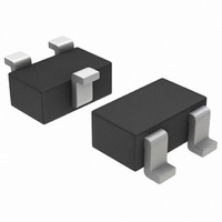
MOSFET P-CH 30V 1.2A SC70-3
Manufacturer
ON Semiconductor
Datasheet
1.NTS4173PT1G.pdf
(6 pages)
Specifications of NTS4173PT1G
Fet Type
MOSFET P-Channel, Metal Oxide
Fet Feature
Logic Level Gate
Rds On (max) @ Id, Vgs
150 mOhm @ 1.2A, 10V
Drain To Source Voltage (vdss)
30V
Current - Continuous Drain (id) @ 25° C
1.2A
Vgs(th) (max) @ Id
1.5V @ 250µA
Gate Charge (qg) @ Vgs
10.1nC @ 10V
Input Capacitance (ciss) @ Vds
430pF @ 15V
Power - Max
290mW
Mounting Type
Surface Mount
Package / Case
SC-70-3, SOT-323-3
Configuration
Single
Transistor Polarity
P-Channel
Resistance Drain-source Rds (on)
0.15 Ohm @ 10 V
Forward Transconductance Gfs (max / Min)
3.6 S
Drain-source Breakdown Voltage
30 V
Gate-source Breakdown Voltage
+/- 12 V
Continuous Drain Current
1.2 A
Power Dissipation
350 mW
Maximum Operating Temperature
+ 150 C
Mounting Style
SMD/SMT
Minimum Operating Temperature
- 55 C
Lead Free Status / RoHS Status
Lead free / RoHS Compliant
Available stocks
Company
Part Number
Manufacturer
Quantity
Price
Company:

Part Number:
NTS4173PT1G
Manufacturer:
ON
Quantity:
9 000
Company:
Part Number:
NTS4173PT1G
Manufacturer:
ON Semiconductor
Quantity:
130
Company:
Part Number:
NTS4173PT1G
Manufacturer:
ON
Quantity:
30 000
Part Number:
NTS4173PT1G
Manufacturer:
ON/安森美
Quantity:
20 000


600
500
400
300
200
100
100
1.0
1.4
1.3
1.2
1.1
1.0
0.9
0.8
0.7
0
10
0
−50
C
1.0
C
rss
V
V
I
Figure 9. Resistive Switching Time Variation
iss
D
GS
DD
C
= −1.2 A
−25
−V
oss
= −4.5 V
= −15 V
5
DS
Figure 7. Capacitance Variation
T
, DRAIN−TO−SOURCE VOLTAGE (V)
J
Figure 11. Threshold Voltage
, JUNCTION TEMPERATURE (°C)
0
R
G
10
vs. Gate Resistance
, GATE RESISTANCE (W)
25
15
10
50
75
20
TYPICAL CHARACTERISTICS
100
I
V
T
f = 1 MHz
D
J
GS
= −250 mA
25
= 25°C
= 0 V
125
http://onsemi.com
t
t
d(off)
t
d(on)
t
f
r
30
100
150
4
12
10
8
6
4
2
0
0
20
18
16
14
12
10
0.0001
1.0
0.1
Q
10
8
6
4
2
0
gs
0.3
Figure 8. Gate−to−Source Voltage vs. Total
Figure 10. Diode Forward Voltage vs. Current
Figure 12. Single Pulse Maximum Power
Q
V
0.001
0.4
gd
DS
2
−V
Q
G
SD
, TOTAL GATE CHARGE (nC)
0.5
T
, SOURCE−TO−DRAIN VOLTAGE (V)
J
0.01
= 150°C
SINGLE PULSE TIME (s)
0.6
4
Charge
Dissipation
0.1
QT
0.7
125°C
6
0.8
1
25°C
0.9
V
I
T
D
V
DS
J
10
T
= −1.2 A
GS
= 25°C
J
8
= −15 V
= −55°C
1.0
100
1.1
10
16
14
12
10
8
6
4
2
0
1000
1.2
Related parts for NTS4173PT1G
Image
Part Number
Description
Manufacturer
Datasheet
Request
R

Part Number:
Description:
SPACER NYL M4/M3THREAD .40"
Manufacturer:
Richco Plastic Co
Datasheet:

Part Number:
Description:
ON Semiconductor [VOLTAGE REGULATOR]
Manufacturer:
ON Semiconductor
Datasheet:
Part Number:
Description:
357-036-542-201 CARDEDGE 36POS DL .156 BLK LOPRO
Manufacturer:
ON Semiconductor
Datasheet:
Part Number:
Description:
357-036-542-201 CARDEDGE 36POS DL .156 BLK LOPRO
Manufacturer:
ON Semiconductor
Datasheet:
Part Number:
Description:
357-036-542-201 CARDEDGE 36POS DL .156 BLK LOPRO
Manufacturer:
ON Semiconductor
Datasheet:
Part Number:
Description:
357-036-542-201 CARDEDGE 36POS DL .156 BLK LOPRO
Manufacturer:
ON Semiconductor
Datasheet:
Part Number:
Description:
357-036-542-201 CARDEDGE 36POS DL .156 BLK LOPRO
Manufacturer:
ON Semiconductor
Datasheet:
Part Number:
Description:
357-036-542-201 CARDEDGE 36POS DL .156 BLK LOPRO
Manufacturer:
ON Semiconductor
Datasheet:
Part Number:
Description:
357-036-542-201 CARDEDGE 36POS DL .156 BLK LOPRO
Manufacturer:
ON Semiconductor
Datasheet:
Part Number:
Description:
357-036-542-201 CARDEDGE 36POS DL .156 BLK LOPRO
Manufacturer:
ON Semiconductor
Datasheet:
Part Number:
Description:
357-036-542-201 CARDEDGE 36POS DL .156 BLK LOPRO
Manufacturer:
ON Semiconductor
Datasheet:
Part Number:
Description:
357-036-542-201 CARDEDGE 36POS DL .156 BLK LOPRO
Manufacturer:
ON Semiconductor
Datasheet:
Part Number:
Description:
Manufacturer:
ON Semiconductor
Datasheet:
Part Number:
Description:
Manufacturer:
ON Semiconductor
Datasheet: