IRFB4310PBF International Rectifier, IRFB4310PBF Datasheet
IRFB4310PBF
Manufacturer Part Number
IRFB4310PBF
Description
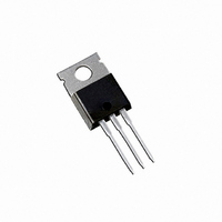
MOSFET N-CH 100V 130A TO-220AB
Manufacturer
International Rectifier
Series
HEXFET®r
Specifications of IRFB4310PBF
Fet Type
MOSFET N-Channel, Metal Oxide
Fet Feature
Standard
Rds On (max) @ Id, Vgs
7 mOhm @ 75A, 10V
Drain To Source Voltage (vdss)
100V
Current - Continuous Drain (id) @ 25° C
130A
Vgs(th) (max) @ Id
4V @ 250µA
Gate Charge (qg) @ Vgs
250nC @ 10V
Input Capacitance (ciss) @ Vds
7670pF @ 50V
Power - Max
300W
Mounting Type
Through Hole
Package / Case
TO-220-3 (Straight Leads)
Current, Drain
130 A
Gate Charge, Total
170 nC
Package Type
TO-220AB
Polarization
N-Channel
Power Dissipation
300 W
Resistance, Drain To Source On
5.6 Milliohms
Temperature, Operating, Maximum
+175 °C
Temperature, Operating, Minimum
-55 °C
Time, Turn-off Delay
68 ns
Time, Turn-on Delay
26 ns
Transconductance, Forward
160 S
Voltage, Breakdown, Drain To Source
100 V
Voltage, Forward, Diode
1.3 V
Voltage, Gate To Source
±20 V
Transistor Polarity
N-Channel
Drain-source Breakdown Voltage
100 V
Gate-source Breakdown Voltage
20 V
Continuous Drain Current
140 A
Mounting Style
Through Hole
Gate Charge Qg
170 nC
Lead Free Status / RoHS Status
Lead free / RoHS Compliant
Other names
*IRFB4310PBF
Available stocks
Company
Part Number
Manufacturer
Quantity
Price
Company:

Part Number:
IRFB4310PBF
Manufacturer:
IR
Quantity:
35 000
Part Number:
IRFB4310PBF
Manufacturer:
IR
Quantity:
20 000


Applications
l
l
l
l
Benefits
l
l
l
l
Absolute Maximum Ratings
I
I
I
P
V
dV/dt
T
T
Avalanche Characteristics
E
I
E
Thermal Resistance
R
R
R
R
D
D
DM
AR
J
STG
D
GS
AS (Thermally limited)
AR
θJC
θCS
θJA
θJA
@ T
@ T
High Efficiency Synchronous Rectification in SMPS
High Speed Power Switching
Uninterruptible Power Supply
Hard Switched and High Frequency Circuits
Improved Gate, Avalanche and Dynamic dV/dt
Ruggedness
Fully Characterized Capacitance and Avalanche
Enhanced body diode dV/dt and dI/dt Capability
Lead-Free
SOA
@T
Symbol
Symbol
C
C
C
= 25°C
= 100°C
= 25°C
Continuous Drain Current, V
Continuous Drain Current, V
Pulsed Drain Current
Maximum Power Dissipation
Linear Derating Factor
Gate-to-Source Voltage
Peak Diode Recovery
Operating Junction and
Storage Temperature Range
Soldering Temperature, for 10 seconds
(1.6mm from case)
Mounting torque, 6-32 or M3 screw
Single Pulse Avalanche Energy
Avalanche Current
Repetitive Avalanche Energy
Junction-to-Case
Case-to-Sink, Flat Greased Surface , TO-220
Junction-to-Ambient, TO-220
Junction-to-Ambient (PCB Mount) , D
Parameter
Parameter
k
Ù
f
GS
GS
g
k
@ 10V
@ 10V
e
2
Pak
jk
G
IRFB4310PbF
TO-220AB
G
D
S
D
S
See Fig. 14, 15, 22a, 22b,
Typ.
0.50
–––
–––
–––
V
R
I
D
DSS
DS(on)
10lb
-55 to + 175
IRFS4310PbF
x
in (1.1N
130
Max.
92
HEXFET Power MOSFET
550
300
± 20
300
980
2.0
D
14
™
2
™
Pak
typ.
G
max.
IRFSL4310PbF
D
x
m)
IRFB4310PbF
IRFS4310PbF
S
Max.
0.50
–––
62
40
5.6m
7.0m
IRFSL4310PbF
100V
130A
TO-262
Units
Units
W/°C
°C/W
V/ns
mJ
mJ
°C
W
A
V
A
G
D
S
1
Related parts for IRFB4310PBF
Image
Part Number
Description
Manufacturer
Datasheet
Request
R

Part Number:
Description:
SCHOTTKY RECTIFIER
Manufacturer:
International Rectifier Corp.
Datasheet:
Part Number:
Description:
SCHOTTKY RECTIFIER
Manufacturer:
International Rectifier Corp.
Datasheet:
Part Number:
Description:
SCHOTTKY RECTIFIER
Manufacturer:
International Rectifier Corp.
Datasheet:
Part Number:
Description:
SCHOTTKY RECTIFIER
Manufacturer:
International Rectifier Corp.
Datasheet:
Part Number:
Description:
SCHOTTKY RECTIFIER
Manufacturer:
International Rectifier Corp.
Datasheet:
Part Number:
Description:
SCHOTTKY RECTIFIER
Manufacturer:
International Rectifier Corp.
Datasheet:
Part Number:
Description:
SCHOTTKY RECTIFIER
Manufacturer:
International Rectifier Corp.
Datasheet:
Part Number:
Description:
SCHOTTKY RECTIFIER
Manufacturer:
International Rectifier Corp.
Datasheet:
Part Number:
Description:
SCHOTTKY RECTIFIER
Manufacturer:
International Rectifier Corp.
Datasheet:
Part Number:
Description:
SCHOTTKY RECTIFIER
Manufacturer:
International Rectifier Corp.
Datasheet:
Part Number:
Description:
SCHOTTKY RECTIFIER
Manufacturer:
International Rectifier Corp.
Datasheet:
Part Number:
Description:
SCHOTTKY RECTIFIER
Manufacturer:
International Rectifier Corp.
Datasheet:
Part Number:
Description:
SCHOTTKY RECTIFIER
Manufacturer:
International Rectifier Corp.
Datasheet:
Part Number:
Description:
SCHOTTKY RECTIFIER
Manufacturer:
International Rectifier Corp.
Datasheet:
Part Number:
Description:
SCHOTTKY RECTIFIER
Manufacturer:
International Rectifier Corp.
Datasheet:
IRFB4310PBF Summary of contents
Page 1
... Junction-to-Case θJC R Case-to-Sink, Flat Greased Surface , TO-220 θCS R Junction-to-Ambient, TO-220 θJA R Junction-to-Ambient (PCB Mount θJA G TO-220AB IRFB4310PbF Parameter @ 10V GS @ 10V Ù g Parameter Pak IRFB4310PbF IRFS4310PbF IRFSL4310PbF HEXFET Power MOSFET D V DSS R typ. 5.6m DS(on) max. 7. Pak IRFS4310PbF IRFSL4310PbF Max. ™ ...
Page 2
Static @ T = 25°C (unless otherwise specified) J Symbol Parameter V Drain-to-Source Breakdown Voltage (BR)DSS ∆V /∆T Breakdown Voltage Temp. Coefficient (BR)DSS J R Static Drain-to-Source On-Resistance DS(on) V Gate Threshold Voltage GS(th) I Drain-to-Source Leakage Current DSS I ...
Page 3
TO-220AB packages are not recommended for Surface Mount Application. 8 ...