IRFP4710PBF International Rectifier, IRFP4710PBF Datasheet
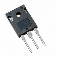
MOSFET N-CH 100V 72A TO-247AC

IRFP4710PBF

Manufacturer Part Number
IRFP4710PBF
Description
MOSFET N-CH 100V 72A TO-247AC
Manufacturer
International Rectifier
Series
HEXFET®r
Type
Power MOSFETr
Datasheets

Specifications of IRFP4710PBF

Fet Type
MOSFET N-Channel, Metal Oxide
Fet Feature
Standard
Rds On (max) @ Id, Vgs
14 mOhm @ 45A, 10V
Drain To Source Voltage (vdss)
100V
Current - Continuous Drain (id) @ 25° C
72A
Vgs(th) (max) @ Id
5.5V @ 250µA
Gate Charge (qg) @ Vgs
170nC @ 10V
Input Capacitance (ciss) @ Vds
6160pF @ 25V
Power - Max
190W
Mounting Type
Through Hole
Package / Case
TO-247-3 (Straight Leads), TO-247AC
Current, Drain
72 A
Gate Charge, Total
110 nC
Package Type
TO-247AC
Polarization
N-Channel
Power Dissipation
190 W
Resistance, Drain To Source On
0.011 Ohm
Temperature, Operating, Maximum
+175 °C
Temperature, Operating, Minimum
-55 °C
Time, Turn-off Delay
41 ns
Time, Turn-on Delay
35 ns
Transconductance, Forward
35 S
Voltage, Breakdown, Drain To Source
100 V
Voltage, Forward, Diode
1.3 V
Voltage, Gate To Source
±20 V
Number Of Elements
1
Polarity
N
Channel Mode
Enhancement
Drain-source On-res
0.014Ohm
Drain-source On-volt
100V
Gate-source Voltage (max)
±20V
Continuous Drain Current
72A
Operating Temp Range
-55C to 175C
Operating Temperature Classification
Military
Mounting
Through Hole
Pin Count
3 +Tab
Transistor Polarity
N-Channel
Drain-source Breakdown Voltage
100 V
Gate-source Breakdown Voltage
20 V
Mounting Style
Through Hole
Gate Charge Qg
110 nC
Lead Free Status / RoHS Status
Lead free / RoHS Compliant
Other names
*IRFP4710PBF

Available stocks

Company
Part Number
Manufacturer
Quantity
Price
Part Number:
IRFP4710PBF
Manufacturer:
NEC
Quantity:
10 000
Company:
Part Number:
IRFP4710PBF
Quantity:
5 000
l
l
l
l
l
l
l
Thermal Resistance
www.irf.com
Applications
Absolute Maximum Ratings
Notes 
Benefits
I
I
I
P
V
dv/dt
T
T
R
R
R
D
D
DM
J
STG
D
GS
θJC
θCS
θJA
@ T
@ T
Effective C
App. Note AN1001)
and Current
High frequency DC-DC converters
Motor Control
Uninterruptible Power Supplies
Lead-Free
Low Gate-to-Drain Charge to Reduce
Fully Characterized Capacitance Including
Fully Characterized Avalanche Voltage
@T
Switching Losses
C
C
C
= 25°C
= 100°C
= 25°C
through …
OSS
Continuous Drain Current, V
Pulsed Drain Current 
Power Dissipation
Linear Derating Factor
Gate-to-Source Voltage
Peak Diode Recovery dv/dt ƒ
Operating Junction and
Storage Temperature Range
Soldering Temperature, for 10 seconds
Mounting torqe, 6-32 or M3 screw
Junction-to-Case
Case-to-Sink, Flat, Greased Surface
Junction-to-Ambient
to Simplify Design, (See
are on page 8
Parameter
Parameter
GS
GS
@ 10V
@ 10V
V
100V
DSS
Typ.
300 (1.6mm from case )
0.24
–––
–––
IRFP4710PbF
10 lbf•in (1.1N•m)
HEXFET Power MOSFET
-55 to + 175
R
Max.
300
190
± 20
1.2
8.2
DS(on)
72
51
0.014Ω
Max.
0.81
max
–––
40
TO-247AC
PD - 95055
Units
Units
W/°C
°C/W
V/ns
72A
°C
W
I
A
V
D
1

Related parts for IRFP4710PBF

IRFP4710PBF Summary of contents

Page 1

... Thermal Resistance Parameter R Junction-to-Case θJC R Case-to-Sink, Flat, Greased Surface θCS R Junction-to-Ambient θJA Notes  through … are on page 8 www.irf.com IRFP4710PbF HEXFET Power MOSFET V R DSS 100V Max. @ 10V GS @ 10V GS - 175 300 (1.6mm from case ) 10 lbf•in (1.1N•m) Typ. ––– ...

Page 2

... IRFP4710PbF Static @ T = 25°C (unless otherwise specified) J Parameter V Drain-to-Source Breakdown Voltage (BR)DSS ∆V Breakdown Voltage Temp. Coefficient /∆T (BR)DSS J R Static Drain-to-Source On-Resistance DS(on) V Gate Threshold Voltage GS(th) I Drain-to-Source Leakage Current DSS Gate-to-Source Forward Leakage I GSS Gate-to-Source Reverse Leakage Dynamic @ T = 25°C (unless otherwise specified) ...

Page 3

... Fig 2. Typical Output Characteristics 3 2.5 2.0 1.5 1.0 0.5 = 50V 0.0 9.0 10.0 -60 -40 -20 0 Fig 4. Normalized On-Resistance IRFP4710PbF VGS 15V 12V 10V 8.0V 7.5V 7.0V 6.5V 6.0V 6.0V 20µs PULSE WIDTH ° 175 Drain-to-Source Voltage (V) DS 75A ...

Page 4

... IRFP4710PbF 10000 0V MHZ C iss = rss = C gd 8000 C oss = Ciss 6000 4000 2000 Coss Crss Drain-to-Source Voltage (V) Fig 5. Typical Capacitance Vs. Drain-to-Source Voltage 1000 100 T = 175 C ° 0.1 0.0 0.4 0.8 V ,Source-to-Drain Voltage (V) SD Fig 7. Typical Source-Drain Diode Forward Voltage SHORTED 100 0 0 Fig 6. Typical Gate Charge Vs. ...

Page 5

... Fig 11. Maximum Effective Transient Thermal Impedance, Junction-to-Case www.irf.com Fig 10a. Switching Time Test Circuit V DS 90% 125 150 175 ° 10 Fig 10b. Switching Time Waveforms 0.001 0. Rectangular Pulse Duration (sec) 1 IRFP4710PbF + - ≤ 1 ≤ 0 d(on) r d(off Notes: 1. Duty factor ...

Page 6

... IRFP4710PbF D.U 20V V GS 0.01 Ω Fig 12a. Unclamped Inductive Test Circuit V (BR)DSS Fig 12b. Unclamped Inductive Waveforms Charge Fig 13a. Basic Gate Charge Waveform 6 350 15V 300 DRIVER 250 + 200 150 100 Starting T , Junction Temperature ( C) Fig 12c. Maximum Avalanche Energy Fig 13b ...

Page 7

... Waveform DS Re-Applied Voltage Inductor Curent Fig 14. For N-Channel HEXFET www.irf.com + • • ƒ • - „ • • • • P.W. Period D = Period Body Diode Forward Current di/dt Diode Recovery dv/dt Body Diode Forward Drop Ripple ≤ 5% ® Power MOSFETs IRFP4710PbF + - V =10V ...

Page 8

... IRFP4710PbF 15.90 (.626) 15.30 (.602 20.30 (.800) 19.70 (.775 14.80 (.583) 14.20 (.559) 2.40 (.094) 2.00 (.079 5.45 (.215) 3.40 (.133) 2X 3.00 (.118) EXAMPLE: T HIS IS AN IRFPE30 WIT H ASSEMBLY LOT CODE 5657 ASSEMBLED ON WW 35, 2000 IN THE AS SEMBLY LINE "H" Note: "P" in assembly line position indicates " ...

Page 9

Note: For the most current drawings please refer to the IR website at: http://www.irf.com/package/ ...

Related keywords