IRFB3307ZGPBF International Rectifier, IRFB3307ZGPBF Datasheet
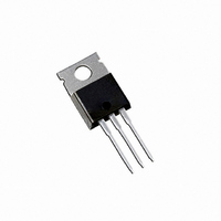
IRFB3307ZGPBF
Specifications of IRFB3307ZGPBF


Related parts for IRFB3307ZGPBF


IRFB3307ZGPBF Summary of contents
Page 1
... Parameter j IRFB3307ZGPbF HEXFET Power MOSFET V 75V DSS R typ. 4.6m DS(on) max. 5.8m I 120A D (Silicon Limited) I 120A D (Package Limited TO-220AB IRFB3307ZGPbF Gate Drain Source Max. ™ 120 84 120 480 230 1.5 ± 20 6.7 - 175 300 x x 10lbf in (1.1N m) 140 See Fig. 14, 15, 22a, 22b Typ ...
Page 2
Static @ T = 25°C (unless otherwise specified) J Symbol Parameter V Drain-to-Source Breakdown Voltage (BR)DSS ∆V /∆T Breakdown Voltage Temp. Coefficient (BR)DSS J R Static Drain-to-Source On-Resistance DS(on) V Gate Threshold Voltage GS(th) R Internal Gate Resistance G(int) I ...
Page 3
VGS TOP 15V 10V 8.0V 6.0V 5.5V 5.0V 100 4.8V BOTTOM 4.5V 4.5V 10 ≤ 60µs PULSE WIDTH Tj = 25° Drain-to-Source Voltage (V) Fig 1. Typical Output Characteristics 1000 100 T J ...
Page 4
175°C 100 25° 0.1 0.0 0.5 1 Source-to-Drain Voltage (V) Fig 7. Typical Source-Drain Diode Forward Voltage 120 100 100 ...
Page 5
D = 0.50 0.20 0.1 0.10 0.05 0.02 0.01 0.01 SINGLE PULSE ( THERMAL RESPONSE ) 0.001 1E-006 Fig 13. Maximum Effective Transient Thermal Impedance, Junction-to-Case 100 0.01 0.05 10 0.10 1 Allowed avalanche Current vs avalanche pulsewidth, tav, ...
Page 6
150µA 2 250µA 1 1.0mA 1.0A 1.0 0.5 -75 -50 - 100 125 150 175 200 ...
Page 7
D.U.T + ƒ ‚ - R • • • SD • Fig 20 D.U 20V V GS 0.01 Ω Fig 21a. Unclamped Inductive Test Circuit ...
Page 8
TO-220AB packages are not recommended for Surface Mount Application. IR WORLD HEADQUARTERS: 233 Kansas St., El Segundo, California 90245, USA Tel: (310) 252-7105 8 Data and specifications subject to change without notice. This product has been designed and qualified for ...