IRLH5030TR2PBF International Rectifier, IRLH5030TR2PBF Datasheet
Home Discrete Semiconductor Products MOSFETs, GaNFETs - Single IRLH5030TR2PBF
Manufacturer Part Number
IRLH5030TR2PBF
Description
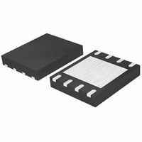
MOSFET N-CH 100V 13A 8VQFN
Manufacturer
International Rectifier
Specifications of IRLH5030TR2PBF
Fet Type
MOSFET N-Channel, Metal Oxide
Fet Feature
Logic Level Gate
Rds On (max) @ Id, Vgs
9 mOhm @ 50A, 10V
Drain To Source Voltage (vdss)
100V
Current - Continuous Drain (id) @ 25° C
13A
Vgs(th) (max) @ Id
2.5V @ 150µA
Gate Charge (qg) @ Vgs
94nC @ 10V
Input Capacitance (ciss) @ Vds
5185pF @ 50V
Power - Max
3.6W
Mounting Type
Surface Mount
Package / Case
8-VQFN
Transistor Polarity
N-Channel
Resistance Drain-source Rds (on)
9.9 mOhms
Drain-source Breakdown Voltage
100 V
Gate-source Breakdown Voltage
16 V
Continuous Drain Current
13 A
Power Dissipation
3.6 W
Gate Charge Qg
44 nC
Number Of Elements
1
Polarity
N
Channel Mode
Enhancement
Drain-source On-res
0.009Ohm
Drain-source On-volt
100V
Gate-source Voltage (max)
±16V
Operating Temp Range
-55C to 150C
Operating Temperature Classification
Military
Mounting
Surface Mount
Pin Count
8
Lead Free Status / RoHS Status
Lead free / RoHS Compliant
Other names
IRLH5030TR2PBFTR
Available stocks
Part Number:
IRLH5030TR2PBF
Applications
•
•
•
•
Features and Benefits
www.irf.com
Features
Notes through
Orderable part number
IRLH5030TRPBF
IRLH5030TR2PBF
Low R
Low Thermal Resistance to PCB (≤ 0.5°C/W)
100% Rg tested
Low Profile (≤ 0.9 mm)
Industry-Standard Pinout
Compatible with Existing Surface Mount Techniques
RoHS Compliant Containing no Lead, no Bromide and no Halogen
MSL1, Industrial Qualification
V
V
I
I
I
I
I
P
P
T
T
Absolute Maximum Ratings
D
D
D
D
DM
J
STG
DS
GS
D
D
Secondary Side Synchronous Rectification
Inverters for DC Motors
DC-DC Brick Applications
Boost Converters
@ T
@ T
@ T
@ T
@T
@ T
A
A
C(Bottom)
C(Bottom)
A
(@T
DSon
C(Bottom)
= 25°C
= 70°C
= 25°C
(@V
R
R
Q
(≤9.0mΩ)
c(Bottom)
DS(on) max
G (typical)
g (typical)
= 25°C
= 100°C
GS
= 25°C
V
I
DS
D
= 4.5V)
†
= 25°C)
are on page 8
Drain-to-Source Voltage
Gate-to-Source Voltage
Continuous Drain Current, V
Continuous Drain Current, V
Continuous Drain Current, V
Continuous Drain Current, V
Pulsed Drain Current c
Power Dissipation g
Power Dissipation g
Linear Derating Factor g
Operating Junction and
Storage Temperature Range
PQFN 5mm x 6mm
PQFN 5mm x 6mm
Package Type
100h
100
9.9
1.2
44
Parameter
mΩ
nC
Ω
A
V
GS
GS
GS
GS
@ 10V
@ 10V
@ 10V h
@ 10V
Tape and Reel
Tape and Reel
Form
Standard Pack
results in Increased Power Density
⇒
IRLH5030PbF
Benefits
Increased Reliability
Lower Conduction Losses
Enable better thermal dissipation
Multi-Vendor Compatibility
Easier Manufacturing
Environmentally Friendlier
Increased Reliability
HEXFET
Quantity
-55 to + 150
4000
1000
0.029
Max.
100
100
400
250
±16
3.6
13
11
70
®
PQFN 5X6 mm
Power MOSFET
Note
01/08/2010
Units
W/°C
°C
W
V
A
1
Related parts for IRLH5030TR2PBF
IRLH5030TR2PBF Summary of contents
... Low Profile (≤ 0.9 mm) Industry-Standard Pinout Compatible with Existing Surface Mount Techniques RoHS Compliant Containing no Lead, no Bromide and no Halogen MSL1, Industrial Qualification Orderable part number IRLH5030TRPBF PQFN 5mm x 6mm IRLH5030TR2PBF PQFN 5mm x 6mm Absolute Maximum Ratings V Drain-to-Source Voltage DS V Gate-to-Source Voltage ...
Static @ T = 25°C (unless otherwise specified) J Parameter BV Drain-to-Source Breakdown Voltage DSS ∆ΒV /∆T Breakdown Voltage Temp. Coefficient DSS J R Static Drain-to-Source On-Resistance DS(on) V Gate Threshold Voltage GS(th) ∆V Gate Threshold Voltage Coefficient GS(th) I ...
VGS TOP 10V 5.0V 4.5V 3.5V 3.3V 3.0V 2.9V BOTTOM 2.7V 100 2. Drain-to-Source Voltage (V) Fig 1. Typical Output Characteristics 1000 100 25° 25V ...
150°C 100 10 1 0.1 0.0 0.2 0.4 0 Source-to-Drain Voltage (V) Fig 7. Typical Source-Drain Diode Forward Voltage 120 Limited By Package 100 ...
V GS, Gate -to -Source Voltage (V) Fig 12. On-Resistance vs. Gate Voltage D.U 20V 0.01 Ω Fig 14a. Unclamped Inductive ...
D.U.T + ƒ • • - • + ‚ - • • • SD • Fig 16. DUT Fig 17. Gate Charge Test Circuit 6 Driver Gate Drive P.W. D.U.T. I Waveform SD Reverse Recovery „ ...
PQFN 5x6 Outline "B" Package Details For footprint and stencil design recommendations, please refer to application note AN-1154 at http://www.irf.com/technical-info/appnotes/an-1154.pdf PQFN 5x6 Outline "B" Part Marking DATE CODE ASSEMBLY SITE CODE (Per SCOP 200-002) IDENTIFIER Note: For the most current ...
... Qualification standards can be found at International Rectifier’s web site http://www.irf.com/product-info/reliability †† Higher qualification ratings may be available should the user have such requirements. Please contact your International Rectifier sales representative for further information: http://www.irf.com/whoto-call/salesrep/ ††† Applicable version of JEDEC standard at the time of product release. ...
Related keywords
irlh5030trpbf irlh5030tr2pbf IRLH5030TR2PBF datasheet IRLH5030TR2PBF data sheet IRLH5030TR2PBF pdf datasheet IRLH5030TR2PBF component IRLH5030TR2PBF part IRLH5030TR2PBF distributor IRLH5030TR2PBF RoHS IRLH5030TR2PBF datasheet download