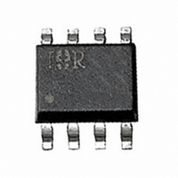
IRF7493PBF International Rectifier, IRF7493PBF Datasheet

IRF7493PBF
Specifications of IRF7493PBF
Available stocks
Related parts for IRF7493PBF
IRF7493PBF Summary of contents
Page 1
... Junction-to-Ambient R θJA Notes through … are on page 9 www.irf.com V DSS 15m @V 80V Top View @ 10V GS @ 10V Typ. ––– f ––– IRF7493PbF ® HEXFET Power MOSFET R max Qg (typ.) DS(on) =10V 35nC SO-8 Max. Units 80 V ± 20 9.3 7.4 ...
Page 2
... IRF7493PbF Static @ T = 25°C (unless otherwise specified) J Parameter BV Drain-to-Source Breakdown Voltage DSS ∆ΒV /∆T Breakdown Voltage Temp. Coefficient DSS J R Static Drain-to-Source On-Resistance DS(on) V Gate Threshold Voltage GS(th) I Drain-to-Source Leakage Current DSS I Gate-to-Source Forward Leakage GSS Gate-to-Source Reverse Leakage Dynamic @ T = 25° ...
Page 3
... Fig 3. Typical Transfer Characteristics www.irf.com 100 10 1 0.1 10 100 0.1 Fig 2. Typical Output Characteristics 2 9. 10V 1.5 1.0 0.5 5.0 6.0 -60 -40 -20 Fig 4. Normalized On-Resistance IRF7493PbF 3.5V 20µs PULSE WIDTH Tj = 150° Drain-to-Source Voltage ( 100 120 140 160 Junction Temperature (°C) Vs. Temperature 100 3 ...
Page 4
... IRF7493PbF 100000 0V MHZ C iss = rss = oss = 10000 Ciss 1000 Coss Crss 100 Drain-to-Source Voltage (V) Fig 5. Typical Capacitance Vs. Drain-to-Source Voltage 100 150°C 10.0 1 25°C 0.1 0.2 0.4 0.6 0 Source-toDrain Voltage (V) Fig 7. Typical Source-Drain Diode Forward Voltage 5.6A SHORTED 100 Fig 6. Typical Gate Charge Vs. ...
Page 5
... SINGLE PULSE ( THERMAL RESPONSE ) 0.01 1E-005 0.0001 Fig 11. Maximum Effective Transient Thermal Impedance, Junction-to-Ambient www.irf.com Fig 10a. Switching Time Test Circuit V DS 90% 125 150 10 d(on) Fig 10b. Switching Time Waveforms 0.001 0.01 0 Rectangular Pulse Duration (sec) IRF7493PbF + - ≤ 1 ≤ 0 d(off 100 5 ...
Page 6
... IRF7493PbF 0.013 0.012 10V 0.011 Drain Current (A) Fig 12. On-Resistance Vs. Drain Current Current Regulator Same Type as D.U. 50KΩ .2µF 12V .3µ D.U. 3mA Current Sampling Resistors Fig 14a&b. Basic Gate Charge Test Circuit and Waveform V (BR)DSS 20V Fig 15a&b. Unclamped Inductive Test circuit ...
Page 7
... SD Reverse „ Recovery Current - + D.U.T. V Waveform DS Re-Applied G + Voltage - Inductor Curent ® HEXFET Power MOSFETs Qgd Qgodr Fig 17. Gate Charge Waveform IRF7493PbF P.W. Period D = Period V =10V GS Body Diode Forward Current di/dt Diode Recovery dv/ Body Diode Forward Drop I Ripple ≤ for N-Channel Id Vgs ...
Page 8
... IRF7493PbF SO-8 Package Outline Dimensions are shown in millimeters (inches 0.25 [.010 NOT DIMENS IONING & TOLERANCING PER ASME Y14.5M-1994. 2. CONT ROLLING DIMENS ION: MILLIMET ER 3. DIMENS IONS ARE SHOWN IN MILLIMETERS [INCHES]. 4. OUTLINE CONFORMS TO JEDEC OUTLINE MS -012AA. 5 DIMENS ION DOES NOT INCLUDE MOLD PROT RUSIONS . ...
Page 9
... V oss DS Data and specifications subject to change without notice. Qualifications Standards can be found on IR’s Web site. Visit us at www.irf.com for sales contact information.09/04 IRF7493PbF 12.3 ( .484 ) 11.7 ( .461 ) 14.40 ( .566 ) 12.40 ( .488 ) DSS TAC Fax: (310) 252-7903 ...


