IRF7410TRPBF International Rectifier, IRF7410TRPBF Datasheet
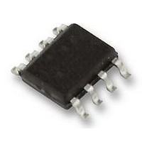
MOSFET P-CH 12V 16A 8-SOIC

IRF7410TRPBF

Manufacturer Part Number
IRF7410TRPBF
Description
MOSFET P-CH 12V 16A 8-SOIC
Manufacturer
International Rectifier
Series
HEXFET®r
Datasheet

Specifications of IRF7410TRPBF

Package / Case
8-SOIC (3.9mm Width)
Mounting Type
Surface Mount
Power - Max
2.5W
Fet Type
MOSFET P-Channel, Metal Oxide
Gate Charge (qg) @ Vgs
91nC @ 4.5V
Vgs(th) (max) @ Id
900mV @ 250µA
Current - Continuous Drain (id) @ 25° C
16A
Drain To Source Voltage (vdss)
12V
Fet Feature
Logic Level Gate
Rds On (max) @ Id, Vgs
7 mOhm @ 16A, 4.5V
Transistor Polarity
P Channel
Continuous Drain Current Id
16A
Drain Source Voltage Vds
12V
On Resistance Rds(on)
7mohm
Rds(on) Test Voltage Vgs
4.5V
Threshold Voltage Vgs Typ
900mV
Rohs Compliant
Yes
Resistance Drain-source Rds (on)
7 mOhms
Drain-source Breakdown Voltage
- 12 V
Gate-source Breakdown Voltage
8 V
Continuous Drain Current
- 16 A
Power Dissipation
2.5 W
Mounting Style
SMD/SMT
Gate Charge Qg
91 nC
Lead Free Status / RoHS Status
Lead free / RoHS Compliant

Available stocks

Company
Part Number
Manufacturer
Quantity
Price
Part Number:
IRF7410TRPBF
Manufacturer:
AMD
Quantity:
1 390
Part Number:
IRF7410TRPBF
Manufacturer:
IR
Quantity:
20 000
Part Number:
IRF7410TRPBF
0
Company:
Part Number:
IRF7410TRPBF
Quantity:
3 850
Company:
Part Number:
IRF7410TRPBF
Quantity:
24 000
Company:
Part Number:
IRF7410TRPBF
Quantity:
68 000
l
l
l
l
Thermal Resistance
These P-Channel HEXFET
International Rectifier utilize advanced processing
techniques to achieve the extremely low on-resistance
per silicon area. This benefit provides the designer
with an extremely efficient device for use in battery
and load management applications..
The SO-8 has been modified through a customized
leadframe for enhanced thermal characteristics and
multiple-die capability making it ideal in a variety of
power applications. With these improvements, multiple
devices can be used in an application with dramatically
reduced board space. The package is designed for
vapor phase, infrared, or wave soldering technique
Description
www.irf.com
R
V
I
I
I
P
P
V
T
D
D
DM
DS
D
D
GS
J,
θJA
@ T
@ T
Ultra Low On-Resistance
P-Channel MOSFET
Surface Mount
Available in Tape & Reel
T
@T
@T
STG
A
A
A
A
= 70°C
= 25°C
= 25°C
= 70°C
Maximum Junction-to-Ambient
Drain- Source Voltage
Continuous Drain Current, V
Pulsed Drain Current 
Power Dissipation
Power Dissipation
Linear Derating Factor
Gate-to-Source Voltage
Junction and Storage Temperature Range
®
Power MOSFETs from
Parameter
Parameter
ƒ
ƒ
GS
GS
ƒ
@ -4.5V
@ -4.5V
G
S
S
S
V
-12V
DSS
1
2
3
4
Top View
HEXFET Power MOSFET
13mΩ@V
7mΩ@V
9mΩ@V
8
6
5
7
-55 to +150
R
Max.
Max.
DS(on)
50
D
D
D
D
-12
-16
-13
-65
2.5
1.6
A
20
±8
GS
GS
GS
IRF7410
max
= -4.5V
= -2.5V
= -1.8V
SO-8
-
-
13.6A
11.5A
-
16A
mW/°C
Units
Units
I
°C/W
D
°C
V
A
V
1
8/2/06

Related parts for IRF7410TRPBF

IRF7410TRPBF Summary of contents

Page 1

... Description ® These P-Channel HEXFET Power MOSFETs from International Rectifier utilize advanced processing techniques to achieve the extremely low on-resistance per silicon area. This benefit provides the designer with an extremely efficient device for use in battery and load management applications.. The SO-8 has been modified through a customized ...

Page 2

Electrical Characteristics @ T Parameter V Drain-to-Source Breakdown Voltage (BR)DSS Breakdown Voltage Temp. Coefficient ∆V /∆T (BR)DSS J R Static Drain-to-Source On-Resistance DS(on) V Gate Threshold Voltage GS(th) g Forward Transconductance fs I Drain-to-Source Leakage Current DSS Gate-to-Source Forward Leakage ...

Page 3

PULSE WIDTH Tj = 25°C 0.1 0 Drain-to-Source Voltage (V) Fig 1. Typical Output Characteristics 100 ° 150 ° ...

Page 4

0V MHZ C iss = SHORTED 12000 C rss = oss = 10000 Ciss 8000 6000 4000 ...

Page 5

T , Case Temperature Fig 9. Maximum Drain Current Vs. Case Temperature 100 D = 0.50 0.20 10 0.10 0.05 0.02 1 0.01 SINGLE PULSE 0.1 (THERMAL RESPONSE) 0.01 ...

Page 6

-16A 0.004 0.002 0.0 2.0 4.0 -V GS, Gate -to -Source Voltage (V) Fig 12. Typical On-Resistance Vs. Gate Voltage Charge Fig 14a. Basic Gate Charge ...

Page 7

Temperature ( °C ) Fig 15. Typical Vgs(th) Vs. Junction Temperature www.irf.com 700 600 500 400 -250µA 300 200 100 0 0.0001 0.0010 ...

Page 8

SO-8 Package Details 0.25 [.010 NOT DIMENS IONING & T OLERANCING PER AS ME ...

Page 9

Tape and Reel TERMINAL NUMBER 1 8.1 ( .318 ) 7.9 ( .312 ) NOTES: 1. CONTROLLING DIMENSION : MILLIMETER. 2. ALL DIMENSIONS ARE SHOWN IN MILLIMETERS(INCHES). 3. OUTLINE CONFORMS TO EIA-481 & EIA-541. NOTES : 1. CONTROLLING DIMENSION : ...

Related keywords