IRF730A Vishay, IRF730A Datasheet - Page 4
IRF730A
Manufacturer Part Number
IRF730A
Description
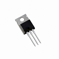
MOSFET N-CH 400V 5.5A TO-220AB
Manufacturer
Vishay
Datasheet
1.IRF730A.pdf
(8 pages)
Specifications of IRF730A
Fet Type
MOSFET N-Channel, Metal Oxide
Fet Feature
Standard
Rds On (max) @ Id, Vgs
1 Ohm @ 3.3A, 10V
Drain To Source Voltage (vdss)
400V
Current - Continuous Drain (id) @ 25° C
5.5A
Vgs(th) (max) @ Id
4.5V @ 250µA
Gate Charge (qg) @ Vgs
22nC @ 10V
Input Capacitance (ciss) @ Vds
600pF @ 25V
Power - Max
74W
Mounting Type
Through Hole
Package / Case
TO-220-3 (Straight Leads)
Configuration
Single
Transistor Polarity
N-Channel
Resistance Drain-source Rds (on)
1 Ohms
Drain-source Breakdown Voltage
400 V
Gate-source Breakdown Voltage
+/- 30 V
Continuous Drain Current
5.5 A
Power Dissipation
74 W
Maximum Operating Temperature
+ 150 C
Mounting Style
Through Hole
Minimum Operating Temperature
- 55 C
Lead Free Status / RoHS Status
Contains lead / RoHS non-compliant
Other names
*IRF730A
Available stocks
Company
Part Number
Manufacturer
Quantity
Price

Company:
Part Number:
IRF730A
Manufacturer:
IR
Quantity:
12 500
Part Number:
IRF730A
Manufacturer:
IR
Quantity:
20 000
Company:
Part Number:
IRF730AL
Manufacturer:
IR
Quantity:
12 500
Company:
Part Number:
IRF730APBF
Manufacturer:
VISHAY
Quantity:
20 000
Part Number:
IRF730APBF
Manufacturer:
VISHAY/威世
Quantity:
20 000
Company:
Part Number:
IRF730AS
Manufacturer:
IR
Quantity:
12 500


IRF730A, SiHF730A
Vishay Siliconix
www.vishay.com
4
91045_05
91045_06
Fig. 5 - Typical Capacitance vs. Drain-to-Source Voltage
Fig. 6 - Typical Gate Charge vs. Gate-to-Source Voltage
10
10
10
10
10
20
16
12
1
8
4
0
5
4
3
2
1
0
I
D
= 5.5 A
V
DS ,
5
Q
G
Drain-to-Source Voltage (V)
V
, Total Gate Charge (nC)
DS
10
V
= 80 V
DS
10
V
C
C
C
= 200 V
GS
iss
rss
oss
V
= C
= 0 V, f = 1 MHz
= C
DS
= C
= 320 V
gs
gd
15
ds
+ C
+ C
10
2
gd
gd
For test circuit
see figure 13
, C
C
C
C
iss
oss
rss
ds
20
Shorted
10
25
3
91045_08
91045_07
Fig. 7 - Typical Source-Drain Diode Forward Voltage
10
0.1
10
0.1
10
10
1
1
2
2
10
0.4
Fig. 8 - Maximum Safe Operating Area
V
V
DS
SD
Operation in this area limited
T
, Drain-to-Source Voltage (V)
0.6
, Source-to-Drain Voltage (V)
J
= 150
T
T
Single Pulse
C
J
°
by R
= 150 °C
= 25 °C
C
10
0.8
DS(on)
2
T
J
S-83000-Rev. A, 19-Jan-09
= 25
Document Number: 91045
°
C
1.0
V
10
100
1
10
GS
ms
µs
ms
= 0 V
µs
10
1.2
3
Related parts for IRF730A
Image
Part Number
Description
Manufacturer
Datasheet
Request
R

Part Number:
Description:
357-036-542-201 CARDEDGE 36POS DL .156 BLK LOPRO
Manufacturer:
Vishay
Datasheet:
Part Number:
Description:
357-036-542-201 CARDEDGE 36POS DL .156 BLK LOPRO
Manufacturer:
Vishay
Datasheet:
Part Number:
Description:
357-036-542-201 CARDEDGE 36POS DL .156 BLK LOPRO
Manufacturer:
Vishay
Datasheet:
Part Number:
Description:
357-036-542-201 CARDEDGE 36POS DL .156 BLK LOPRO
Manufacturer:
Vishay
Datasheet:
Part Number:
Description:
357-036-542-201 CARDEDGE 36POS DL .156 BLK LOPRO
Manufacturer:
Vishay
Datasheet:
Part Number:
Description:
357-036-542-201 CARDEDGE 36POS DL .156 BLK LOPRO
Manufacturer:
Vishay
Datasheet:
Part Number:
Description:
357-036-542-201 CARDEDGE 36POS DL .156 BLK LOPRO
Manufacturer:
Vishay
Datasheet:
Part Number:
Description:
357-036-542-201 CARDEDGE 36POS DL .156 BLK LOPRO
Manufacturer:
Vishay
Datasheet:
Part Number:
Description:
357-036-542-201 CARDEDGE 36POS DL .156 BLK LOPRO
Manufacturer:
Vishay
Datasheet:
Part Number:
Description:
357-036-542-201 CARDEDGE 36POS DL .156 BLK LOPRO
Manufacturer:
Vishay
Datasheet:
Part Number:
Description:
357-036-542-201 CARDEDGE 36POS DL .156 BLK LOPRO
Manufacturer:
Vishay
Datasheet:
Part Number:
Description:
357-036-542-201 CARDEDGE 36POS DL .156 BLK LOPRO
Manufacturer:
Vishay
Datasheet:
Part Number:
Description:
357-036-542-201 CARDEDGE 36POS DL .156 BLK LOPRO
Manufacturer:
Vishay
Datasheet:
Part Number:
Description:
357-036-542-201 CARDEDGE 36POS DL .156 BLK LOPRO
Manufacturer:
Vishay
Datasheet:
Part Number:
Description:
357-036-542-201 CARDEDGE 36POS DL .156 BLK LOPRO
Manufacturer:
Vishay
Datasheet: