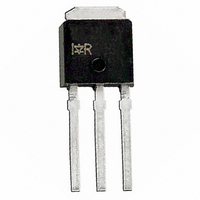
IRLU3714ZPBF International Rectifier, IRLU3714ZPBF Datasheet - Page 8

IRLU3714ZPBF
Manufacturer Part Number
IRLU3714ZPBF
Description
MOSFET N-CH 20V 37A I-PAK
Manufacturer
International Rectifier
Series
HEXFET®r
Datasheet
1.IRLU3714ZPBF.pdf
(12 pages)
Specifications of IRLU3714ZPBF
Fet Type
MOSFET N-Channel, Metal Oxide
Fet Feature
Logic Level Gate
Rds On (max) @ Id, Vgs
15 mOhm @ 15A, 10V
Drain To Source Voltage (vdss)
20V
Current - Continuous Drain (id) @ 25° C
37A
Vgs(th) (max) @ Id
2.55V @ 250µA
Gate Charge (qg) @ Vgs
7.1nC @ 4.5V
Input Capacitance (ciss) @ Vds
560pF @ 10V
Power - Max
35W
Mounting Type
Through Hole
Package / Case
IPak, TO-251, DPak, VPak (3 straight leads + tab)
Transistor Polarity
N Channel
Continuous Drain Current Id
37A
Drain Source Voltage Vds
20V
On Resistance Rds(on)
15mohm
Rds(on) Test Voltage Vgs
10V
Peak Reflow Compatible (260 C)
Yes
Rohs Compliant
Yes
Resistance Drain-source Rds (on)
25 mOhms
Drain-source Breakdown Voltage
20 V
Gate-source Breakdown Voltage
20 V
Continuous Drain Current
37 A
Power Dissipation
35 W
Mounting Style
SMD/SMT
Gate Charge Qg
4.7 nC
Lead Free Status / RoHS Status
Lead free / RoHS Compliant
Other names
*IRLU3714ZPBF
Available stocks
Company
Part Number
Manufacturer
Quantity
Price
Company:
Part Number:
IRLU3714ZPBF
Manufacturer:
IR
Quantity:
4 272
Control FET
P
P
Power MOSFET Selection for Non-Isolated DC/DC Converters
loss
8
loss
This can be expanded and approximated by;
= I
+ I ×
+ Q
+
= P
(
⎛
⎜
⎝
(
⎛
⎝
Q
rms
conduction
g
2
oss
× V
2
Q
× R
i
× V
g
gd
g
× f
ds(on )
in
× V
+ P
× f
)
in
)
switching
× f
⎞
⎠
⎞
⎟ + I ×
⎠
+ P
⎛
⎜
⎝
drive
Q
+ P
i
gs 2
g
× V
output
in
× f
⎞
⎟
⎠
Synchronous FET
by;
*dissipated primarily in Q1.
portant characteristic; however, once again the im-
portance of gate charge must not be overlooked since
it impacts three critical areas. Under light load the
MOSFET must still be turned on and off by the con-
trol IC so the gate drive losses become much more
significant. Secondly, the output charge Q
verse recovery charge Q
are transfered to Q1 and increase the dissipation in
that device. Thirdly, gate charge will impact the
MOSFETs’ susceptibility to Cdv/dt turn on.
of the converter and therefore sees transitions be-
tween ground and V
a rate of change of drain voltage dV/dt which is ca-
pacitively coupled to the gate of Q2 and can induce
a voltage spike on the gate that is sufficient to turn
the MOSFET on, resulting in shoot-through current .
The ratio of Q
potential for Cdv/dt turn on.
Figure A: Q
P
P
loss
loss
The power loss equation for Q2 is approximated
For the synchronous MOSFET Q2, R
The drain of Q2 is connected to the switching node
= P
= I
+ Q
+
(
(
⎛
⎜
⎝
conduction
rms
Q
oss
g
2
oss
2
Characteristic
× V
gd
× R
/Q
× V
g
gs1
+ P
ds(on)
× f
in
in
must be minimized to reduce the
. As Q1 turns on and off there is
drive
× f
)
)
rr
⎞
⎠
+ P
both generate losses that
+ Q
output
(
*
rr
× V
www.irf.com
in
ds(on)
× f
oss
is an im-
and re-
)


