IRLU3715PBF International Rectifier, IRLU3715PBF Datasheet - Page 2
IRLU3715PBF
Manufacturer Part Number
IRLU3715PBF
Description
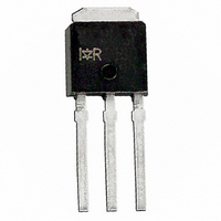
MOSFET N-CH 20V 54A I-PAK
Manufacturer
International Rectifier
Series
HEXFET®r
Datasheet
1.IRLR3715PBF.pdf
(11 pages)
Specifications of IRLU3715PBF
Fet Type
MOSFET N-Channel, Metal Oxide
Fet Feature
Logic Level Gate
Rds On (max) @ Id, Vgs
14 mOhm @ 26A, 10V
Drain To Source Voltage (vdss)
20V
Current - Continuous Drain (id) @ 25° C
54A
Vgs(th) (max) @ Id
3V @ 250µA
Gate Charge (qg) @ Vgs
17nC @ 4.5V
Input Capacitance (ciss) @ Vds
1060pF @ 10V
Power - Max
3.8W
Mounting Type
Through Hole
Package / Case
IPak, TO-251, DPak, VPak (3 straight leads + tab)
Transistor Polarity
N Channel
Continuous Drain Current Id
54A
Drain Source Voltage Vds
20V
On Resistance Rds(on)
14mohm
Rds(on) Test Voltage Vgs
10V
Peak Reflow Compatible (260 C)
Yes
Rohs Compliant
Yes
Resistance Drain-source Rds (on)
20 mOhms
Drain-source Breakdown Voltage
20 V
Gate-source Breakdown Voltage
20 V
Continuous Drain Current
54 A
Power Dissipation
71 W
Mounting Style
SMD/SMT
Gate Charge Qg
11 nC
Lead Free Status / RoHS Status
Lead free / RoHS Compliant
Other names
*IRLU3715PBF
Available stocks
Company
Part Number
Manufacturer
Quantity
Price
Company:

Part Number:
IRLU3715PBF
Manufacturer:
TI
Quantity:
5 354


IRLR/U3715PbF
Diode Characteristics
Dynamic @ T
Avalanche Characteristics
Static @ T
Symbol
E
I
V
∆V
R
V
Symbol
g
Q
Q
Q
Q
t
t
t
t
C
C
C
V
I
Symbol
I
I
t
Q
t
Q
I
AR
d(on)
r
d(off)
f
SM
DSS
S
rr
rr
GSS
2
fs
AS
(BR)DSS
GS(th)
SD
DS(on)
gs
gd
oss
iss
oss
rss
g
rr
rr
(BR)DSS
/∆T
J
Breakdown Voltage Temp. Coefficient
Drain-to-Source Breakdown Voltage
Gate Threshold Voltage
Gate-to-Source Forward Leakage
Gate-to-Source Reverse Leakage
Forward Transconductance
Total Gate Charge
Gate-to-Source Charge
Gate-to-Drain ("Miller") Charge
Output Gate Charge
Turn-On Delay Time
Rise Time
Turn-Off Delay Time
Fall Time
Input Capacitance
Output Capacitance
Reverse Transfer Capacitance
Drain-to-Source Leakage Current
Continuous Source Current
(Body Diode)
Pulsed Source Current
(Body Diode)
Reverse Recovery Time
Reverse Recovery Charge
Reverse Recovery Time
Reverse Recovery Charge
Static Drain-to-Source On-Resistance
Diode Forward Voltage
J
= 25°C (unless otherwise specified)
J
Single Pulse Avalanche Energy‚
Avalanche Current
= 25°C (unless otherwise specified)
Parameter
Parameter
Parameter
Parameter
–––
–––
–––
–––
–––
–––
–––
–––
–––
–––
–––
–––
–––
–––
–––
–––
–––
–––
Min. Typ. Max. Units
Min. Typ. Max. Units
1.0
Min. Typ. Max. Units
20
26
–––
–––
–––
–––
–––
–––
–––
–––
0.022
1060 –––
–––
–––
–––
–––
–––
––– -200
–––
700
120
–––
–––
3.8
4.4
6.4
5.1
0.9
0.8
11
15
11
11
73
12
37
28
38
30
–––
100
200
–––
–––
–––
–––
–––
–––
–––
–––
–––
210
3.0
54
–––
1.3
–––
20
17
17
42
45
56
57
14
20
„
mΩ
V/°C
µA
nA
nC
ns
pF
nC
nC
ns
ns
V
V
S
V
Typ.
–––
–––
I
V
V
V
V
V
V
V
V
V
V
V
V
V
I
R
V
V
V
ƒ = 1.0MHz
T
di/dt = 100A/µs ƒ
T
di/dt = 100A/µs ƒ
MOSFET symbol
showing the
integral reverse
p-n junction diode.
T
T
D
D
Reference to 25°C, I
GS
GS
GS
DS
DS
DS
GS
GS
DS
DS
GS
GS
DD
GS
GS
DS
J
J
J
J
G
= 21A
= 21A
= 25°C, I
= 125°C, I
= 25°C, I
= 125°C, I
= 1.8Ω
= V
= 16V, V
= 16V, V
= 10V, I
= 10V
= 10V
= 0V, I
= 10V, I
= 4.5V, I
= 16V
= -16V
= 4.5V
= 0V, V
= 10V
= 4.5V
= 0V
GS
, I
D
S
F
DS
D
D
D
Conditions
D
= 250µA
S
GS
GS
F
Conditions
Conditions
ƒ
= 21A, V
= 21A, V
= 250µA
= 26A
= 21A
= 21A
= 21A, V
= 21A, V
= 10V
Max.
= 0V
= 0V, T
110
21
www.irf.com
D
GS
R
ƒ
= 1mA
ƒ
=20V
R
J
GS
=20V
= 125°C
= 0V ƒ
G
= 0V ƒ
Units
mJ
A
S
D
Related parts for IRLU3715PBF
Image
Part Number
Description
Manufacturer
Datasheet
Request
R

Part Number:
Description:
SCHOTTKY RECTIFIER
Manufacturer:
International Rectifier Corp.
Datasheet:
Part Number:
Description:
SCHOTTKY RECTIFIER
Manufacturer:
International Rectifier Corp.
Datasheet:
Part Number:
Description:
SCHOTTKY RECTIFIER
Manufacturer:
International Rectifier Corp.
Datasheet:
Part Number:
Description:
SCHOTTKY RECTIFIER
Manufacturer:
International Rectifier Corp.
Datasheet:
Part Number:
Description:
SCHOTTKY RECTIFIER
Manufacturer:
International Rectifier Corp.
Datasheet:
Part Number:
Description:
SCHOTTKY RECTIFIER
Manufacturer:
International Rectifier Corp.
Datasheet:
Part Number:
Description:
SCHOTTKY RECTIFIER
Manufacturer:
International Rectifier Corp.
Datasheet:
Part Number:
Description:
SCHOTTKY RECTIFIER
Manufacturer:
International Rectifier Corp.
Datasheet:
Part Number:
Description:
SCHOTTKY RECTIFIER
Manufacturer:
International Rectifier Corp.
Datasheet:
Part Number:
Description:
SCHOTTKY RECTIFIER
Manufacturer:
International Rectifier Corp.
Datasheet:
Part Number:
Description:
SCHOTTKY RECTIFIER
Manufacturer:
International Rectifier Corp.
Datasheet:
Part Number:
Description:
SCHOTTKY RECTIFIER
Manufacturer:
International Rectifier Corp.
Datasheet:
Part Number:
Description:
SCHOTTKY RECTIFIER
Manufacturer:
International Rectifier Corp.
Datasheet:
Part Number:
Description:
SCHOTTKY RECTIFIER
Manufacturer:
International Rectifier Corp.
Datasheet:
Part Number:
Description:
SCHOTTKY RECTIFIER
Manufacturer:
International Rectifier Corp.
Datasheet: