AO4404B Alpha & Omega Semiconductor Inc, AO4404B Datasheet
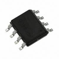
MOSFET N-CH 30V 8.5A 8-SOIC

AO4404B

Manufacturer Part Number
AO4404B
Description
MOSFET N-CH 30V 8.5A 8-SOIC
Manufacturer
Alpha & Omega Semiconductor Inc
Datasheet

Specifications of AO4404B

Fet Type
MOSFET N-Channel, Metal Oxide
Fet Feature
Logic Level Gate
Rds On (max) @ Id, Vgs
24 mOhm @ 8.5A, 10V
Drain To Source Voltage (vdss)
30V
Current - Continuous Drain (id) @ 25° C
8.5A
Vgs(th) (max) @ Id
1.5V @ 250µA
Gate Charge (qg) @ Vgs
12nC @ 4.5V
Input Capacitance (ciss) @ Vds
1100pF @ 15V
Power - Max
2.8W
Mounting Type
Surface Mount
Package / Case
8-SOIC
Lead Free Status / RoHS Status
Lead free / RoHS Compliant
Other names
785-1020-2

Available stocks

Company
Part Number
Manufacturer
Quantity
Price
Part Number:
AO4404B
Manufacturer:
ALPHA
Quantity:
7 823
Part Number:
AO4404B
Manufacturer:
AO
Quantity:
20 000
Part Number:
AO4404BL
Manufacturer:
AOS/万代
Quantity:
20 000
Company:
Part Number:
AO4404BL
Quantity:
590
Rev 2: July 2010
Absolute Maximum Ratings T
Parameter
Drain-Source Voltage
Gate-Source Voltage
Continuous Drain
Current
Pulsed Drain Current
Avalanche Current
Avalanche energy L=0.1mH
Power Dissipation
Junction and Storage Temperature Range
Thermal Characteristics
Maximum Junction-to-Ambient
Maximum Junction-to-Lead
General Description
The AO4404B uses advanced trench technology to
provide excellent R
operation with gate voltages as low as 2.5V. This device
makes an excellent high side switch for notebook CPU
core DC-DC conversion.
D
D
D
D
B
Parameter
C
DS(ON)
C
D
D
Top View
Top View
T
T
T
T
A
A
A
A
D
D
=25° C
=70° C
=25° C
=70° C
, low gate charge and
C
S
S
A
A D
S
S
A
=25° C unless otherwise noted
SOIC-8
SOIC-8
S
S
t ≤ 10s
Steady-State
Steady-State
G
G
Bottom View
Bottom View
Symbol
V
V
V
I
I
I
E
P
T
Symbol
D
DM
AS
www.aosmd.com
DS
DS
GS
AS
D
J
, T
, I
R
R
, E
AR
STG
JA
JL
AR
V
I
R
R
R
100% UIS Tested
100% R
Product Summary
D
DS
DS(ON)
DS(ON)
DS(ON)
(at V
Typ
31
59
16
(at V
(at V
(at V
GS
g
=10V)
Tested
GS
GS
GS
Maximum
-55 to 150
=10V)
= 4.5V)
= 2.5V)
±12
8.5
7.1
3.1
30
30
60
14
10
2
30V N-Channel MOSFET
G
G
Max
40
75
24
D
D
S
S
AO4404B
30V
8.5A
< 24m
< 30m
< 48m
Units
Units
° C/W
° C/W
° C/W
mJ
° C
W
V
V
V
A
A
Page 1 of 6

Related parts for AO4404B

AO4404B Summary of contents

Page 1

... General Description The AO4404B uses advanced trench technology to provide excellent R , low gate charge and DS(ON) operation with gate voltages as low as 2.5V. This device makes an excellent high side switch for notebook CPU core DC-DC conversion. SOIC-8 SOIC-8 Top View Top View Absolute Maximum Ratings T =25° ...

Page 2

... FR-4 board with 2oz. Copper still air environment with T =150°C, using ≤ 10s junction-to-ambient thermal resistance. =150°C. Ratings are based on low frequency and duty cycles to keep J(MAX) and lead to ambient. JL =150°C. The SOA curve provides a single pulse rating. J(MAX) www.aosmd.com AO4404B Min Typ Max Units =55° C ...

Page 3

... Figure 4: On-Resistance vs. Junction Temperature Figure 4: On-Resistance vs. Junction Temperature 1.0E+01 I =8.5A D 1.0E+00 40 1.0E-01 125° 1.0E-02 1.0E-03 1.0E-04 25° 1.0E-05 0 Figure 6: Body-Diode Characteristics (Note E) www.aosmd.com AO4404B V V =5V = 25°C 25°C 125°C 125° 1.5 1 2.5 2 (Volts) (Volts =4.5V =4. =8.5A =8 ...

Page 4

... T T =100°C =100° 1.0 1.0 0.1 0.1 0.0 0.0 0.01 100 100 1000 1000 0. Figure 10: Maximum Forward Biased Safe Figure 10: Maximum Forward Biased Safe 0.1 Pulse Width (s) www.aosmd.com AO4404B C C iss iss oss oss (Volts) (Volts 100 s 100 s 1ms ...

Page 5

... Figure 12: Normalized Maximum Transient Thermal Impedance (Note F) Rev 2: July 2010 In descending order In descending order D=0.5, 0.3, 0.1, 0.05, 0.02, 0.01, single pulse D=0.5, 0.3, 0.1, 0.05, 0.02, 0.01, single pulse 0.01 0.01 0.1 0 Pulse Width (s) Pulse Width (s) www.aosmd.com AO4404B 100 100 1000 1000 Page ...

Page 6

... Vgs Vgs d(on) d( Vds Vds + + Vgs Vgs Vdd VDC Id - Vgs Diode Recovery Test Circuit & Waveforms Idt Vgs Isd Vdd VDC - Vds www.aosmd.com AO4404B Qg Qg Qgd Qgd Charge Charge 90% 90% 10% 10 d(off) d(off off off DSS DSS dI/ Vdd Page ...

Related keywords