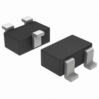
2N7002WT1G ON Semiconductor, 2N7002WT1G Datasheet

MOSFET N-CH SGL 60V 340MA SOT323

2N7002WT1G

Manufacturer Part Number
2N7002WT1G
Description
MOSFET N-CH SGL 60V 340MA SOT323
Manufacturer
ON Semiconductor
Type
Small Signalr
Datasheet

Specifications of 2N7002WT1G

Fet Type
MOSFET N-Channel, Metal Oxide
Fet Feature
Logic Level Gate
Rds On (max) @ Id, Vgs
1.6 Ohm @ 500mA, 10V
Drain To Source Voltage (vdss)
60V
Current - Continuous Drain (id) @ 25° C
310mA
Vgs(th) (max) @ Id
2.5V @ 250µA
Gate Charge (qg) @ Vgs
0.7nC @ 4.5V
Input Capacitance (ciss) @ Vds
24.5pF @ 20V
Power - Max
280mW
Mounting Type
Surface Mount
Package / Case
SC-70-3, SOT-323-3
Configuration
Single
Transistor Polarity
N-Channel
Resistance Drain-source Rds (on)
1.6 Ohm @ 10 V
Drain-source Breakdown Voltage
60 V
Gate-source Breakdown Voltage
+/- 20 V
Continuous Drain Current
0.31 A
Power Dissipation
280 mW
Maximum Operating Temperature
+ 150 C
Mounting Style
SMD/SMT
Minimum Operating Temperature
- 55 C
Number Of Elements
1
Polarity
N
Channel Mode
Enhancement
Drain-source On-res
1.6Ohm
Drain-source On-volt
60V
Gate-source Voltage (max)
±20V
Operating Temp Range
-55C to 150C
Operating Temperature Classification
Military
Mounting
Surface Mount
Pin Count
3
Package Type
SC-70
Lead Free Status / RoHS Status
Lead free / RoHS Compliant
Other names
2N7002WT1G
2N7002WT1GOSTR

Available stocks

Company
Part Number
Manufacturer
Quantity
Price
Part Number:
2N7002WT1G
Manufacturer:
ON Semiconductor
Quantity:
1 350
Part Number:
2N7002WT1G
Manufacturer:
ON
Quantity:
120 000
Part Number:
2N7002WT1G
Manufacturer:
ON
Quantity:
30 000
Part Number:
2N7002WT1G
Manufacturer:
ON/安森美
Quantity:
20 000
Company:
Part Number:
2N7002WT1G
Quantity:
1 934
Company:
Part Number:
2N7002WT1G
Quantity:
4 500
2N7002W
Small Signal MOSFET
60 V, 340 mA, Single, N−Channel, SC−70
Features
Applications
Stresses exceeding Maximum Ratings may damage the device. Maximum
Ratings are stress ratings only. Functional operation above the Recommended
Operating Conditions is not implied. Extended exposure to stresses above the
Recommended Operating Conditions may affect device reliability.
1. Surface−mounted on FR4 board using 1 in sq pad size (Cu area = 1.127 in
© Semiconductor Components Industries, LLC, 2011
April, 2011 − Rev. 4
MAXIMUM RATINGS
THERMAL CHARACTERISTICS
Drain−to−Source Voltage
Gate−to−Source Voltage
Drain Current (Note 1)
Power Dissipation (Note 1)
Pulsed Drain Current (t
Operating Junction and Storage
Temperature Range
Source Current (Body Diode)
Lead Temperature for Soldering Purposes
Gate−Source ESD Rating
(HBM, Method 3015)
Junction−to−Ambient − Steady State
(Note 1)
Junction−to−Ambient − t ≤ 5 s (Note 1)
Compliant
ESD Protected
Low R
Small Footprint Surface Mount Package
These Devices are Pb−Free, Halogen Free/BFR Free and are RoHS
Low Side Load Switch
Level Shift Circuits
DC−DC Converter
Portable Applications i.e. DSC, PDA, Cell Phone, etc.
sq [1 oz] including traces)
Steady State
t < 5 s
Steady State
t < 5 s
(1/8″ from case for 10 s)
DS(on)
Characteristic
Rating
p
= 10 ms)
(T
J
= 25°C unless otherwise stated)
T
T
T
T
A
A
A
A
= 25°C
= 85°C
= 25°C
= 85°C
T
Symbol
Symbol
J
V
ESD
R
R
V
, T
I
P
DSS
DM
T
I
I
qJA
qJA
GS
D
S
D
L
STG
−55 to
Value
+150
Max
±20
310
220
340
240
280
330
250
260
900
450
375
1.4
60
1
°C/W
Unit
Unit
mW
mA
mA
°C
°C
V
V
A
V
†For information on tape and reel specifications,
2N7002WT1G
including part orientation and tape sizes, please
refer to our Tape and Reel Packaging Specifications
Brochure, BRD8011/D.
SC−70/SOT−323
V
(BR)DSS
60 V
Device
CASE 419
(Note: Microdot may be in either location)
STYLE 8
Source
Gate
ORDERING INFORMATION
SIMPLIFIED SCHEMATIC
71
M
G
http://onsemi.com
1
2
(Pb−Free)
2.5 W @ 4.5 V
Package
1.6 W @ 10 V
= Device Code
= Date Code
= Pb−Free Package
R
SC−70
DS(on)
(Top View)
Publication Order Number:
MARKING DIAGRAM
& PIN ASSIGNMENT
MAX
1
Gate
3000/Tape & Reel
3
71 MG
Shipping
Drain
Drain
3
G
2N7002W/D
(Note 1)
I
340 mA
Source
D
MAX
2

Related parts for 2N7002WT1G

2N7002WT1G Summary of contents

Page 1

... J STG +150 I 250 260 °C L ESD 900 V 2N7002WT1G Symbol Max Unit †For information on tape and reel specifications, 450 °C/W R qJA including part orientation and tape sizes, please refer to our Tape and Reel Packaging Specifications Brochure, BRD8011/D. R 375 qJA 1 http://onsemi.com ...

Page 2

ELECTRICAL CHARACTERISTICS Parameter OFF CHARACTERISTICS Drain−to−Source Breakdown Voltage Drain−to−Source Breakdown Voltage Temperature Coefficient Zero Gate Voltage Drain Current Gate−to−Source Leakage Current ON CHARACTERISTICS (Note 2) Gate Threshold Voltage Negative Threshold Temperature Coefficient Drain−to−Source On Resistance Forward Transconductance CHARGES AND CAPACITANCES ...

Page 3

9.0 V 8.0 V 1.2 7.0 V 6.0 V 0.8 0 DRAIN−TO−SOURCE VOLTAGE (V) DS Figure 1. On−Region Characteristics 125°C ...

Page 4

C iss 20 C oss 10 C rss GATE−TO−SOURCE OR DRAIN−TO−SOURCE VOLTAGE (V) Figure 7. Capacitance Variation 85° 25° 0.1 0.01 ...

Page 5

... SCALE 10:1 details, please download the ON Semiconductor Soldering and Mounting Techniques Reference Manual, SOLDERRM/D. N. American Technical Support: 800−282−9855 Toll Free USA/Canada Japan: ON Semiconductor, Japan Customer Focus Center 2−9−1 Kamimeguro, Meguro−ku, Tokyo, Japan 153−0051 Phone: 81− ...

Related keywords