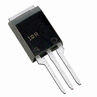
IRFBA90N20DPBF International Rectifier, IRFBA90N20DPBF Datasheet

IRFBA90N20DPBF
Specifications of IRFBA90N20DPBF
Related parts for IRFBA90N20DPBF
IRFBA90N20DPBF Summary of contents
Page 1
... Thermal Resistance Parameter R Junction-to-Case θJC R Case-to-Sink, Flat, Greased Surface θCS R Junction-to-Ambient θJA Notes through † are on page 8 www.irf.com SMPS MOSFET IRFBA90N20DPbF HEXFET V DSS 200V @ 10V GS @ 10V GS - 175 300 (1.6mm from case ) Typ. ––– 0.50 ––– 95902 ® ...
Page 2
... IRFBA90N20DPbF Static @ T = 25°C (unless otherwise specified) J Parameter V Drain-to-Source Breakdown Voltage (BR)DSS ∆V Breakdown Voltage Temp. Coefficient /∆T (BR)DSS J R Static Drain-to-Source On-Resistance DS(on) V Gate Threshold Voltage GS(th) I Drain-to-Source Leakage Current DSS Gate-to-Source Forward Leakage I GSS Gate-to-Source Reverse Leakage Dynamic @ T = 25°C (unless otherwise specified) ...
Page 3
... Drain-to-Source Voltage (V) Fig 1. Typical Output Characteristics 1000.00 100.00 10. 25°C 1. 15V 20µs PULSE WIDTH 0.10 5.0 7.0 9.0 11 Gate-to-Source Voltage (V) Fig 3. Typical Transfer Characteristics www.irf.com IRFBA90N20DPbF 1000 TOP 100 BOTTOM 5. 100 0.1 Fig 2. Typical Output Characteristics 3.5 98A 3 175° ...
Page 4
... IRFBA90N20DPbF 100000 0V MHZ C iss = rss = oss = 10000 Ciss Coss 1000 Crss 100 Drain-to-Source Voltage (V) Fig 5. Typical Capacitance Vs. Drain-to-Source Voltage 1000. 175°C 100. 25°C 10.00 1.00 0.10 0.0 0.5 1.0 1 Source-toDrain Voltage (V) Fig 7. Typical Source-Drain Diode Forward Voltage 4 12 59A SHORTED 10 ...
Page 5
... RESPONSE) 0.001 0.00001 0.0001 Fig 11. Maximum Effective Transient Thermal Impedance, Junction-to-Case www.irf.com Fig 10a. Switching Time Test Circuit V DS 90% 125 150 175 ° 10 Fig 10b. Switching Time Waveforms 0.001 0. Rectangular Pulse Duration (sec) 1 IRFBA90N20DPbF + - ≤ 1 ≤ 0 d(on) r d(off Notes: 1. Duty factor ...
Page 6
... IRFBA90N20DPbF D.U 20V 0.01 Ω Fig 12a. Unclamped Inductive Test Circuit V (BR)DSS Fig 12b. Unclamped Inductive Waveforms Charge Fig 13a. Basic Gate Charge Waveform 6 2000 15V DRIVER 1600 + 1200 800 400 Starting T , Junction Temperature Fig 12c. Maximum Avalanche Energy Fig 13b. Gate Charge Test Circuit ...
Page 7
... D.U.T + ‚ - Driver Gate Drive P.W. D.U.T. I Waveform SD Reverse Recovery Current D.U.T. V Waveform DS Re-Applied Voltage Inductor Curent Fig 14. For N-Channel HEXFET www.irf.com IRFBA90N20DPbF + • • ƒ • - „ • • • • P.W. Period D = Period Body Diode Forward Current di/dt ...
Page 8
... IRFBA90N20DPbF 11.00 [.433] A 10.00 [.394] 1.50 [.059] 0.50 [.020] 15.00 [.590] 14.00 [.552 4.00 [.157] 14.50 [.570] 3.50 [.138] 13.00 [.512] 1.30 [.051] 3X 0.90 [.036] 2.55 [.100] 0.25 [.010] 2X Notes: Repetitive rating; pulse width limited by max. junction temperature. ‚ Starting T = 25° ...
Page 9
... TOP Data and specifications subject to change without notice. This product has been designed and qualified for the Industrial market. Qualification Standards can be found on IR’s Web site. Visit us at www.irf.com for sales contact information.09/04 IRFBA90N20DPbF PART NUMBER 719C 89 DATE CODE YEAR 7 = 1997 ...


