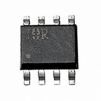
IRF7495PBF International Rectifier, IRF7495PBF Datasheet

IRF7495PBF
Specifications of IRF7495PBF
Related parts for IRF7495PBF
IRF7495PBF Summary of contents
Page 1
... Junction-to-Ambient (PCB Mount) R θJA Notes through † are on page 8 www.irf.com V DSS 22m @V 100V Top View Parameter @ 10V GS @ 10V GS h Parameter Typ. ––– e ––– IRF7495PbF ® HEXFET Power MOSFET R max I DS(on 10V 7. SO-8 Max. Units 100 V ± ...
Page 2
... IRF7495PbF Static @ T = 25°C (unless otherwise specified) J Parameter V Drain-to-Source Breakdown Voltage (BR)DSS ∆V /∆T Breakdown Voltage Temp. Coefficient (BR)DSS J R Static Drain-to-Source On-Resistance DS(on) V Gate Threshold Voltage GS(th) I Drain-to-Source Leakage Current DSS I Gate-to-Source Forward Leakage GSS Gate-to-Source Reverse Leakage Dynamic @ T = 25°C (unless otherwise specified) ...
Page 3
... Fig 2. Typical Output Characteristics 2 7. 10V 2.0 1.5 1.0 0 -60 -40 -20 0 Fig 4. Normalized On-Resistance IRF7495PbF VGS TOP 15V 10V 8.0V 5.0V 4.5V BOTTOM 4.5V 20µs PULSE WIDTH Tj = 150° 100 Drain-to-Source Voltage ( 100 120 140 160 180 Junction Temperature (° ...
Page 4
... IRF7495PbF 100000 0V MHZ C iss = SHORTED C rss = oss = 10000 C iss 1000 C oss C rss 100 Drain-to-Source Voltage (V) Fig 5. Typical Capacitance vs. Drain-to-Source Voltage 100.00 10. 150°C 1. 25°C 0.10 0.01 0.0 0.2 0.4 0 Source-to-Drain Voltage (V) Fig 7. Typical Source-Drain Diode Forward Voltage 4 12 4.4A 10.0 8 ...
Page 5
... SINGLE PULSE ( THERMAL RESPONSE ) 0.01 1E-006 1E-005 0.0001 Fig 11. Maximum Effective Transient Thermal Impedance, Junction-to-Case www.irf.com Fig 10a. Switching Time Test Circuit V DS 90% 125 150 10 d(on) Fig 10b. Switching Time Waveforms 0.001 0.01 0 Rectangular Pulse Duration (sec) IRF7495PbF + - ≤ 1 ≤ 0 d(off 100 5 ...
Page 6
... IRF7495PbF 10V Drain Current (A) Fig 12. On-Resistance vs. Drain Current VCC DUT 0 1K Fig 14a&b. Basic Gate Charge Test Circuit and Waveform V (BR)DSS 20V Fig 15a&b. Unclamped Inductive Test circuit and Waveforms Fig 13. On-Resistance vs. Gate Voltage Q G 500 400 Charge 300 200 15V ...
Page 7
... L 7 6.46 [.255] 3X 1.27 [.050] DATE CODE (YWW DESIGNATES LEAD-FREE PRODUCT (OPTIONAL LAS T DIGIT OF THE YEAR WW = WEEK XXXX A = ASSEMBLY SITE CODE F7101 LOT CODE PART NUMBER IRF7495PbF INCHES MILLIMETERS DIM MIN MAX MIN MAX A .0532 .0688 1.35 1.75 A1 .0040 .0098 ...
Page 8
... IRF7495PbF SO-8 Tape and Reel 8.1 ( .318 ) 7.9 ( .312 ) NOTES: 1. CONTROLLING DIMENSION : MILLIMETER. 2. ALL DIMENSIONS ARE SHOWN IN MILLIMETERS(INCHES). 3. OUTLINE CONFORMS TO EIA-481 & EIA-541. NOTES : 1. CONTROLLING DIMENSION : MILLIMETER. 2. OUTLINE CONFORMS TO EIA-481 & EIA-541. Notes: Repetitive rating; pulse width limited by max. junction temperature. ...


