RUE003N02TL Rohm Semiconductor, RUE003N02TL Datasheet - Page 2
RUE003N02TL
Manufacturer Part Number
RUE003N02TL
Description
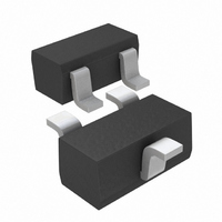
MOSFET N-CH 20V 300MA EMT3
Manufacturer
Rohm Semiconductor
Specifications of RUE003N02TL
Fet Type
MOSFET N-Channel, Metal Oxide
Fet Feature
Logic Level Gate
Rds On (max) @ Id, Vgs
1 Ohm @ 300mA, 4V
Drain To Source Voltage (vdss)
20V
Current - Continuous Drain (id) @ 25° C
300mA
Vgs(th) (max) @ Id
1V @ 1mA
Input Capacitance (ciss) @ Vds
25pF @ 10V
Power - Max
150mW
Mounting Type
Surface Mount
Package / Case
SC-75-3, SOT-416, EMT3, 3-SSMini
Transistor Polarity
N Channel
Drain Source Voltage Vds
20V
On Resistance Rds(on)
700mohm
Rds(on) Test Voltage Vgs
4V
Voltage Vgs Max
8V
Transistor Case Style
EMT
No. Of Pins
3
Svhc
No SVHC
Configuration
Single
Resistance Drain-source Rds (on)
1 Ohm @ 4 V
Drain-source Breakdown Voltage
20 V
Gate-source Breakdown Voltage
+/- 8 V
Continuous Drain Current
0.3 A
Power Dissipation
150 mW
Maximum Operating Temperature
+ 150 C
Mounting Style
SMD/SMT
Minimum Operating Temperature
- 55 C
Lead Free Status / RoHS Status
Lead free / RoHS Compliant
Gate Charge (qg) @ Vgs
-
Lead Free Status / Rohs Status
Lead free / RoHS Compliant
Other names
RUE003N02TLTR
Available stocks
Company
Part Number
Manufacturer
Quantity
Price

Part Number:
RUE003N02TL
Manufacturer:
ROHM/罗姆
Quantity:
20 000


Transistor
∗ Pulsed
∗ Pulsed
Forward voltage
Static drain-source on-state
resistance
Fig.1 Typical transfer characteristics
Electrical characteristics (Ta=25°C)
Gate-source leakage
Drain-source breakdown voltage
Zero gate voltage drain current
Gate threshold voltage
Forward transfer admittance
Input capacitance
Output capacitance
Reverse transfer capacitance
Turn-on delay time
Rise time
Turn-off delay time
Fall time
Body diode characteristics (Source-drain) (Ta=25°C)
Electrical characteristic curves
0.0001
0.00001
0.001
0.01
0.1
0.0
1
V
Pulsed
DS
GATE-SOURCE VOLTAGE : V
=10V
Parameter
Parameter
0.5
1.0
Ta=125°C
−25°C
75°C
25°C
GS
Symbol
(V)
V
V
Symbol
R
SD
V
(BR)DSS
t
t
I
I
|Y
C
C
C
DS(on)
GS(th)
d(on)
d(off)
1.5
GSS
DSS
∗
t
t
oss
rss
iss
fs
r
f
|
∗
∗
∗
∗
∗
∗
Min.
−
Fig.2 Static drain-source on-state
Min.
400
0.3
20
0.1
−
−
−
−
−
−
−
−
−
−
−
−
10
0.01
1
Typ.
−
resistance vs. drain current (Ι)
Ta=125°C
Typ.
0.7
0.8
1.0
25
10
10
10
15
10
−
−
−
−
−
5
DRAIN CURRENT : I
−25°C
Max.
75°C
25°C
1.2
Max.
1.0
1.0
1.0
1.2
1.4
10
−
−
−
−
−
−
−
−
−
0.1
Unit
V
Unit
ms
µA
µA
pF
pF
pF
ns
ns
ns
ns
I
Ω
Ω
Ω
V
V
S
D
= 100mA, V
(A)
V
Pulsed
GS
V
I
V
V
I
I
I
I
V
V
f=1MHz
I
V
R
R
D
D
D
D
D
D
=4V
GS
DS
DS
DS
GS
GS
L
G
=1mA, V
=300mA, V
=300mA, V
=300mA, V
=300mA, V
=150mA, V
=67Ω
=10Ω
=20V, V
=10V, I
=10V
=±8V, V
=0V
=4.0V
Conditions
1
GS
=0V
Fig.3 Static drain-source on-state
GS
D
DS
GS
0.1
=1mA
10
Conditions
=0V
GS
GS
GS
DS
DD
1
0.01
=0V
=0V
=10V
=4.0V
=2.5V
=1.8V
resistance vs. drain current (ΙΙ)
10V
Ta=125°C
DRAIN CURRENT : I
−25°C
75°C
25°C
RUM003N02
Rev.B
0.1
D
(A)
V
Pulsed
GS
=2.5V
2/3
1
Related parts for RUE003N02TL
Image
Part Number
Description
Manufacturer
Datasheet
Request
R

Part Number:
Description:
Manufacturer:
Rohm Semiconductor
Datasheet:
Part Number:
Description:
Manufacturer:
Rohm Semiconductor
Datasheet:
Part Number:
Description:
Manufacturer:
Rohm Semiconductor
Datasheet:
Part Number:
Description:
Manufacturer:
Rohm Semiconductor
Datasheet:
Part Number:
Description:
Manufacturer:
Rohm Semiconductor
Datasheet:
Part Number:
Description:
Manufacturer:
Rohm Semiconductor
Datasheet:
Part Number:
Description:
Manufacturer:
Rohm Semiconductor
Datasheet:
Part Number:
Description:
Manufacturer:
Rohm Semiconductor
Datasheet:
Part Number:
Description:
Manufacturer:
Rohm Semiconductor
Datasheet:
Part Number:
Description:
Manufacturer:
Rohm Semiconductor
Datasheet:
Part Number:
Description:
Manufacturer:
Rohm Semiconductor
Datasheet:
Part Number:
Description:
Manufacturer:
Rohm Semiconductor
Datasheet:

Part Number:
Description:
DIODE SWITCH 80V 25MA SMD5 TR
Manufacturer:
Rohm Semiconductor
Datasheet: