IRFP350LCPBF Vishay, IRFP350LCPBF Datasheet

MOSFET N-CH 400V 16A TO-247AC

IRFP350LCPBF

Manufacturer Part Number
IRFP350LCPBF
Description
MOSFET N-CH 400V 16A TO-247AC
Manufacturer
Vishay
Datasheets

Specifications of IRFP350LCPBF

Transistor Polarity
N-Channel
Fet Type
MOSFET N-Channel, Metal Oxide
Fet Feature
Standard
Rds On (max) @ Id, Vgs
300 mOhm @ 9.6A, 10V
Drain To Source Voltage (vdss)
400V
Current - Continuous Drain (id) @ 25° C
16A
Vgs(th) (max) @ Id
4V @ 250µA
Gate Charge (qg) @ Vgs
76nC @ 10V
Input Capacitance (ciss) @ Vds
2200pF @ 25V
Power - Max
190W
Mounting Type
Through Hole
Package / Case
TO-247-3 (Straight Leads), TO-247AC
Minimum Operating Temperature
- 55 C
Configuration
Single
Resistance Drain-source Rds (on)
0.3 Ohm @ 10 V
Drain-source Breakdown Voltage
400 V
Gate-source Breakdown Voltage
+/- 30 V
Continuous Drain Current
16 A
Power Dissipation
190000 mW
Maximum Operating Temperature
+ 150 C
Mounting Style
Through Hole
Continuous Drain Current Id
16A
Drain Source Voltage Vds
400V
On Resistance Rds(on)
300mohm
Rds(on) Test Voltage Vgs
10V
Threshold Voltage Vgs Typ
4V
Lead Free Status / RoHS Status
Lead free / RoHS Compliant
Lead Free Status / RoHS Status
Lead free / RoHS Compliant, Lead free / RoHS Compliant
Other names
*IRFP350LCPBF
Notes
a. Repetitive rating; pulse width limited by maximum junction temperature (see fig. 11).
b. V
c. I
d. 1.6 mm from case.
* Pb containing terminations are not RoHS compliant, exemptions may apply
Document Number: 91224
S11-0448-Rev. B, 14-Mar-11
THE PRODUCT DESCRIBED HEREIN AND THIS DATASHEET ARE SUBJECT TO SPECIFIC DISCLAIMERS, SET FORTH AT
PRODUCT SUMMARY
V
R
Q
Q
Q
Configuration
ORDERING INFORMATION
Package
Lead (Pb)-free
SnPb
ABSOLUTE MAXIMUM RATINGS (T
PARAMETER
Drain-Source Voltage
Gate-Source Voltage
Continuous Drain Current
Pulsed Drain Current
Linear Derating Factor
Single Pulse Avalanche Energy
Repetitive Avalanche Current
Repetitive Avalanche Energy
Maximum Power Dissipation
Peak Diode Recovery dV/dt
Operating Junction and Storage Temperature Range
Soldering Recommendations (Peak Temperature)
Mounting Torque
DS
DS(on)
g
gs
gd
SD
DD
(Max.) (nC)
(nC)
TO-247AC
(V)
(nC)
≤ 16 A, dI/dt ≤ 200 A/μs, V
= 25 V, starting T
(Ω)
D
a
J
= 25 °C, L = 2.7 mH, R
c
a
a
b
DD
V
GS
≤ V
= 10 V
DS
G
, T
J
N-Channel MOSFET
Single
≤ 150 °C.
400
76
20
37
This datasheet is subject to change without notice.
g
= 25 Ω, I
C
D
S
= 25 °C, unless otherwise noted)
Power MOSFET
0.30
V
GS
AS
6-32 or M3 screw
at 10 V
= 16 A (see fig. 12).
T
for 10 s
C
= 25 °C
T
T
C
C
TO-247AC
IRFP350LCPbF
SiHFP350LC-E3
IRFP350LC
SiHFP350LC
= 100 °C
= 25 °C
FEATURES
• Ultra Low Gate Charge
• Reduced Gate Drive Requirement
• Enhanced 30V V
• Reduced C
• Isolated Central Mounting Hole
• Dynamic dV/dt Rated
• Repetitive Avalanche Rated
• Compliant to RoHS Directive 2002/95/EC
DESCRIPTION
This new series of low charge Power MOSFETs achieve
significantly lower gate charge over conventional MOSFETs.
Utilizing advanced MOSFETs technology the device
improvements allow for reduced gate drive requirements,
faster switching speeds and increased total system savings.
These device improvements combined with the proven
ruggedness and reliability of MOSFETs offer the designer a
new
applications.
The
commercial-industrial applications where higher power
levels preclude the use of TO-220AB devices. The
TO-247AC is similar but superior to the earlier TO-218
package because of its isolated mounting hole.
standard
TO-247AC
SYMBOL
T
dV/dt
IRFP350LC, SiHFP350LC
J
V
iss
V
E
E
I
I
P
, T
DM
I
AR
DS
GS
AR
D
AS
D
, C
stg
oss
in
GS
, C
Rating
power
package
rss
- 55 to + 150
LIMIT
transistors
300
± 30
400
390
190
9.9
1.5
4.0
1.1
16
64
16
19
10
www.vishay.com/doc?91000
d
Vishay Siliconix
is
preferred
for
www.vishay.com
lbf · in
switching
UNIT
W/°C
N · m
V/ns
RoHS*
COMPLIANT
mJ
mJ
°C
W
V
A
A
Available
for
1

Related parts for IRFP350LCPBF

IRFP350LCPBF Summary of contents

Page 1

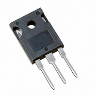
... The TO-247AC N-Channel MOSFET commercial-industrial applications where higher power levels preclude the use of TO-220AB devices. The TO-247AC is similar but superior to the earlier TO-218 package because of its isolated mounting hole. TO-247AC IRFP350LCPbF SiHFP350LC-E3 IRFP350LC SiHFP350LC = 25 °C, unless otherwise noted) C SYMBOL °C ...

Page 2

... IRFP350LC, SiHFP350LC Vishay Siliconix THERMAL RESISTANCE RATINGS PARAMETER Maximum Junction-to-Ambient Case-to-Sink, Flat, Greased Surface Maximum Junction-to-Case (Drain) SPECIFICATIONS ( °C, unless otherwise noted) J PARAMETER Static Drain-Source Breakdown Voltage V Temperature Coefficient DS Gate-Source Threshold Voltage Gate-Source Leakage Zero Gate Voltage Drain Current Drain-Source On-State Resistance ...

Page 3

... Document Number: 91224 S11-0448-Rev. B, 14-Mar-11 THE PRODUCT DESCRIBED HEREIN AND THIS DATASHEET ARE SUBJECT TO SPECIFIC DISCLAIMERS, SET FORTH AT IRFP350LC, SiHFP350LC = 25 °C Fig Typical Transfer Characteristics C Fig Normalized On-Resistance vs. Temperature = 150 °C C This datasheet is subject to change without notice. Vishay Siliconix www.vishay.com 3 www.vishay.com/doc?91000 ...

Page 4

... IRFP350LC, SiHFP350LC Vishay Siliconix Fig Typical Capacitance vs. Drain-to-Source Voltage Fig Typical Gate Charge vs. Gate-to-Source Voltage www.vishay.com 4 THE PRODUCT DESCRIBED HEREIN AND THIS DATASHEET ARE SUBJECT TO SPECIFIC DISCLAIMERS, SET FORTH AT Fig Typical Source-Drain Diode Forward Voltage Fig Maximum Safe Operating Area This datasheet is subject to change without notice. ...

Page 5

... Fig Maximum Effective Transient Thermal Impedance, Junction-to-Case Document Number: 91224 S11-0448-Rev. B, 14-Mar-11 THE PRODUCT DESCRIBED HEREIN AND THIS DATASHEET ARE SUBJECT TO SPECIFIC DISCLAIMERS, SET FORTH AT IRFP350LC, SiHFP350LC Fig. 10a - Switching Time Test Circuit Fig. 10b - Switching Time Waveforms This datasheet is subject to change without notice. Vishay Siliconix D.U. Pulse width ≤ ...

Page 6

... IRFP350LC, SiHFP350LC Vishay Siliconix Vary t to obtain p required I AS D.U 0.01 Ω Fig. 12a - Unclamped Inductive Test Circuit Fig. 12c - Maximum Avalanche Energy vs. Drain Current Charge Fig. 13a - Basic Gate Charge Waveform www.vishay.com 6 THE PRODUCT DESCRIBED HEREIN AND THIS DATASHEET ARE SUBJECT TO SPECIFIC DISCLAIMERS, SET FORTH AT ...

Page 7

... Note a. V Vishay Siliconix maintains worldwide manufacturing capability. Products may be manufactured at one of several qualified locations. Reliability data for Silicon Technology and Package Reliability represent a composite of all qualified locations. For related documents such as package/tape drawings, part marking, and reliability data, see www.vishay.com/ppg?91224. ...

Page 8

... Vishay product could result in personal injury or death. Customers using or selling Vishay products not expressly indicated for use in such applications their own risk and agree to fully indemnify and hold Vishay and its distributors harmless from and against any and all claims, liabilities, expenses and damages arising or resulting in connection with such use or sale, including attorneys fees, even if such claim alleges that Vishay or its distributor was negligent regarding the design or manufacture of the part ...

Related keywords