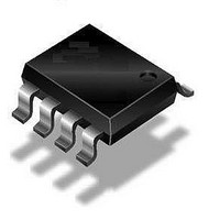
ATA6660-TAPY19 Atmel, ATA6660-TAPY19 Datasheet - Page 3

ATA6660-TAPY19
Manufacturer Part Number
ATA6660-TAPY19
Description
Network Controller & Processor ICs High Speed CAN Transceiver
Manufacturer
Atmel
Datasheet
1.ATA6660-TAQY_19.pdf
(13 pages)
Specifications of ATA6660-TAPY19
Product
Controller Area Network (CAN)
Number Of Transceivers
1
Data Rate
1 MBd
Supply Voltage (max)
6 V
Supply Voltage (min)
- 0.3 V
Supply Current (max)
60 mA
Maximum Operating Temperature
+ 125 C
Minimum Operating Temperature
- 40 C
Mounting Style
SMD/SMT
Package / Case
SO-8
3. Functional Description
3.1
3.2
3.3
3.4
3.5
4582E–AUTO–02/08
Voltage Protection and ESD
Slope Control
Overcurrent Protection
Standby Mode
High-speed Receiver
The ATA6660 is a monolithic circuit based on Atmel’s Smart Power BCD60-III technology. It is
especially designed for high-speed differential mode data transmission in harsh environments
like automotive and industrial applications. Baudrate can be adjusted up to 1 Mbaud. The
ATA6660 is fully compatible to the ISO11898, the developed standard for high speed CAN-C
(Controller Area Network) communication.
High voltage protection circuitry on both line pins, CANH (pin 7) and CANL (pin 6), allow bus line
voltages in the range of –40V to +40V. ESD protection circuitry on line pins allow HBM = 8 kV,
MM = 300V. The implemented high voltage protection on bus line output/input pins (7/6) makes
the ATA6660 suitable for 12V automotive applications as well as 24V automotive applications.
A fixed slope is adjusted to prevent unsymmetrical transients on bus lines causing EMC prob-
lems. Controlled bus lines, both CANH and CANL signal, will reduce radio frequency
interference to a minimum. In well designed bus configurations the filter design costs can be
reduced dramatically.
In the case of a line shorts, like CANH to GND, CANL to VCC, integrated short current limitation
allows a maximum current of I
internal overtemperature protection circuitry shuts down both output stages, the receiver will
stay activated.
The ATA6660 can be switched to Standby Mode by forcing the voltage VRS > 0.87
Standby Mode the supply current will reduce dramatically, supply current during Standby Mode
is typical 600 µA (I
will remain to receive data. A high-speed comparator is listening for activities on the bus. A dom-
inant bus signal will force the output RXD to a low level in typical t
not connected, causing through a broken connection to the controller, the ATA6660 will switch to
Standby Mode automatically.
In Normal Mode a fast receiver circuitry combined with a resistor network is able to detect differ-
ential bus line voltages V
as recessive bit.
The wide receiver common mode range, –10V to +10V, combined with a symmetrical differential
receiver stage offers high immunity against electromagnetic interference. A typical hysteresis of
70 mV is implemented. Dominant differential bus voltages forces RXD output (pin 4) to low level,
recessive differential bus voltages to high level.
VCC_stby
rec_th
). Transmitting data function will not be supported, but the opportunity
> 0.9V as dominant bit, differential bus line voltages V
CANH_SC
or I
CANL_SC
. If junction temperature rises above 165°C an
dRXDL
= 400 ns. If the RS pin is
ATA6660
rec_th
VCC. In
< 0.5V
3


