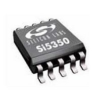
Si5350A-A-GT Silicon Laboratories Inc, Si5350A-A-GT Datasheet - Page 12

Si5350A-A-GT
Manufacturer Part Number
Si5350A-A-GT
Description
Clock Generators & Support Products Any-Rate Dual PLL 125MHz Clk 3 outputs
Manufacturer
Silicon Laboratories Inc
Type
Any Frequency CMOS Clock Generatorr
Datasheet
1.SI5350A-A-GM.pdf
(20 pages)
Specifications of Si5350A-A-GT
Mounting Style
SMD/SMT
Max Input Freq
0.008 MHz
Max Output Freq
125 MHz
Number Of Outputs
3
Operating Supply Voltage
3.3 V
Operating Temperature Range
- 40 C to + 85 C
Supply Current
20 mA
Package / Case
MSOP-10
Lead Free Status / RoHS Status
Lead free / RoHS Compliant
Si5350A
4.4. Design Considerations
The Si5350A is a self-contained clock generator that requires very few external components. The following general
guidelines are recommended to ensure optimum performance.
4.4.1. Power Supply Decoupling/Filtering
The Si5350A has built-in power supply filtering circuitry to help keep the number of external components to a
minimum. All that is recommended is one 0.1 µF decoupling capacitor per power supply pin. This capacitor should
be mounted as close to the VDD and VDDO pins as possible without using vias.
4.4.2. Power Supply Sequencing
The VDD and VDDOx (i.e., VDDO0, VDDO1, VDDO2, VDDO3) power supply pins have been separated to allow
flexibility in output signal levels. It is important that power is applied to all supply pins (VDD, VDDOx) at the same
time. Unused VDDOx pins should be tied to VDD.
4.4.3. External Crystal
The external crystal should be mounted as close to the pins as possible using short PCB traces. The XA and XB
traces should be kept away from other high-speed signal traces. See “AN551: Crystal Selection Guide” for more
details.
4.4.4. External Crystal Load Capacitors
The Si5350A provides the option of using internal and external crystal load capacitors. If external load capacitors
are used, they should be placed as close to the XA/XB pads as possible. See “AN551: Crystal Selection Guide” for
more details.
4.4.5. Unused Pins
Unused control pins (P0–P4) should be tied to GND.
Unused output pins (CLK0–CLK7) should be left floating.
12
Rev. 0.2


