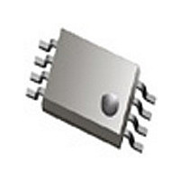
MC10EP89DT ON Semiconductor, MC10EP89DT Datasheet

MC10EP89DT
Specifications of MC10EP89DT
Available stocks
Related parts for MC10EP89DT
MC10EP89DT Summary of contents
Page 1
MC10EP89 3.3V / 5V ECL Coaxial Cable Driver Description The MC10EP89 is a differential fanout gate specifically designed to drive coaxial cables. The device is especially useful in digital video broadcasting applications; for this application, since the system is polarity free, ...
Page 2
Figure 1. 8-Lead Pinout (Top View) and Logic Diagram Table 2. ATTRIBUTES Characteristics Internal Input Pulldown Resistor Internal Input Pullup Resistor ESD Protection Moisture Sensitivity, Indefinite Time Out of Drypack (Note 1) ...
Page 3
Table 3. MAXIMUM RATINGS Symbol Parameter V PECL Mode Power Supply CC V NECL Mode Power Supply EE V PECL Mode Input Voltage I NECL Mode Input Voltage I Output Current out T Operating Temperature Range A T Storage Temperature ...
Page 4
Table 4. DC CHARACTERISTICS, PECL Symbol Characteristic I Power Supply Current EE V Output HIGH Voltage (Note Output LOW Voltage (Note Input HIGH Voltage (Single-Ended Input LOW Voltage (Single-Ended Input ...
Page 5
Table 6. DC CHARACTERISTICS, NECL Symbol Characteristic Power Supply Current IEE V Output HIGH Voltage (Note Output LOW Voltage (Note Input HIGH Voltage (Single-Ended Input LOW Voltage (Single-Ended Input HIGH ...
Page 6
Table 8. AC CHARACTERISTICS V Symbol Characteristic f Maximum Toggle max (See Figure 2 F /JITTER) max t , Propagation Delay to PLH t Output Differential PHL t Within Device Skew SKEW Device to Device Skew (Note 15) t Cycle-to-Cycle ...
Page 7
MC10EP89 DC BLOCKING CAPACITORS EP89 150 Figure 3. Cable Driver Termination Configuration = Driver Device = Figure 4. Typical Termination for Output Driver and Device Evaluation (See ...
Page 8
... ORDERING INFORMATION Device MC10EP89D MC10EP89DG MC10EP89DR2 MC10EP89DR2G MC10EP89DT MC10EP89DTG MC10EP89DTR2 MC10EP89DTR2G MC10EP89MNR4 MC10EP89MNR4G †For information on tape and reel specifications, including part orientation and tape sizes, please refer to our Tape and Reel Packaging Specifications Brochure, BRD8011/D. Resource Reference of Application Notes AN1405/D AN1406/D AN1503/D ...
Page 9
... S B 0.25 (0.010 - SEATING PLANE - 0.25 (0.010 *For additional information on our Pb-Free strategy and soldering details, please download the ON Semiconductor Soldering and Mounting Techniques Reference Manual, SOLDERRM/D. MC10EP89 PACKAGE DIMENSIONS SOIC-8 NB CASE 751-07 ISSUE 0.10 (0.004 SOLDERING FOOTPRINT* 1.52 0.060 7.0 4.0 ...
Page 10
K 8x REF 0.10 (0.004) 0.15 (0.006 L - PIN 1 IDENT 0.15 (0.006 -V- C 0.10 (0.004) -T- D SEATING G PLANE MC10EP89 PACKAGE DIMENSIONS ...
Page 11
... Opportunity/Affirmative Action Employer. This literature is subject to all applicable copyright laws and is not for resale in any manner. PUBLICATION ORDERING INFORMATION LITERATURE FULFILLMENT: Literature Distribution Center for ON Semiconductor P.O. Box 5163, Denver, Colorado 80217 USA Phone: 303-675-2175 or 800-344-3860 Toll Free USA/Canada Fax: 303-675-2176 or 800-344-3867 Toll Free USA/Canada ...


