MC100EP195FA ON Semiconductor, MC100EP195FA Datasheet - Page 4
MC100EP195FA
Manufacturer Part Number
MC100EP195FA
Description
Delay Lines / Timing Elements 3.3V/5V ECL
Manufacturer
ON Semiconductor
Datasheet
1.MC100EP195FA.pdf
(20 pages)
Specifications of MC100EP195FA
Function
Active Programmable Delay Line
Supply Voltage (min)
+/- 3 V
Maximum Operating Temperature
+ 85 C
Minimum Operating Temperature
- 40 C
Mounting Style
SMD/SMT
Supply Voltage (max)
+/- 3.6 V
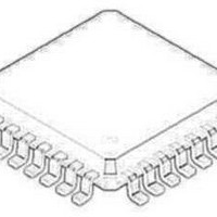
Package / Case
LQFP-32
Lead Free Status / RoHS Status
Lead free / RoHS Compliant
Available stocks
Company
Part Number
Manufacturer
Quantity
Price

Part Number:
MC100EP195FA
Manufacturer:
ON/安森美
Quantity:
20 000
Company:
Part Number:
MC100EP195FAG
Manufacturer:
ON Semiconductor
Quantity:
10 000
Part Number:
MC100EP195FAG
Manufacturer:
ON/安森美
Quantity:
20 000
Company:
Part Number:
MC100EP195FAR2
Manufacturer:
ON Semiconductor
Quantity:
10 000
Company:
Part Number:
MC100EP195FAR2G
Manufacturer:
ON Semiconductor
Quantity:
10 000
Part Number:
MC100EP195FAR2G
Manufacturer:
ON/安森美
Quantity:
20 000


Table 2. CONTROL PIN
3. Internal pulldown resistor will provide a logic LOW if pin is left unconnected.
Table 3. CONTROL D[0:10] INTERFACE
4. Short V
5. When Operating in LVTTL Mode, the reference voltage can be provided by connecting an external resistor, R
is 2.2 kW $5%), between V
SETMAX
SETMIN
LEN
D10
V
V
V
Pin
EN
CF
CF
CF
CF
(pin 8) and V
Table 4. DATA INPUT ALLOWED OPERATING VOLTAGE MODE TABLE
Table 5. ATTRIBUTES
6. For additional information, see Application Note AND8003/D.
Internal Input Pulldown Resistor
ESD Protection
Moisture Sensitivity, Indefinite Time Out of Drypack (Note 6)
Flammability Rating Oxygen Index: 28 to 34
Transistor Count
Meets or exceeds JEDEC Spec EIA/JESD78 IC Latchup Test
PECL Mode Operating Range
NECL Mode Operating Range
EF
V
1.5 V $ 100 mV
(pin 7).
LOW (Note 3)
LOW (Note 3)
LOW (Note 3)
LOW (Note 3)
LOW (Note 3)
EF
CF
POWER SUPPLY
No Connect
Pin (Note 4)
and V
HIGH
HIGH
HIGH
HIGH
HIGH
State
EE
pins.
Characteristics
Input Signal is Propagated to the Output
Output Holds Logic Low State
Transparent or LOAD mode for real time delay values present on D[0:10].
LOCK and HOLD mode for delay values on D[0:10]; further changes on D[0:10]
are not recognized and do not affect delay.
Output Delay set by D[0:10]
Set Minimum Output Delay
Output Delay set by D[0:10]
Set Maximum Output Delay
CASCADE Output LOW, CASCADE Output HIGH
CASCADE Output LOW, CASCADE Output HIGH
ECL Mode
LVCMOS Mode
LVTTL Mode (Note 5)
http://onsemi.com
Charged Device Model
Human Body Model
CONTROL DATA SELECT INPUTS PINS (D [0:10])
LVCMOS
YES
N/A
Machine Model
4
LQFP−32
QFN−32
(R1)
LVTTL
YES
N/A
Pb Pkg
Level 2
UL 94 V−0 @ 0.125 in
LVPECL
Function
−
YES
N/A
1217 Devices
> 100 V
> 2 kV
> 2 kV
Value
75 kW
Pb−Free Pkg
LVNECL
Level 2
Level 1
YES
N/A
CF
(suggested resistor value
Related parts for MC100EP195FA
Image
Part Number
Description
Manufacturer
Datasheet
Request
R

Part Number:
Description:
3.3V / 5VECL Quad 2-Input Differential AND/NAND
Manufacturer:
ON Semiconductor
Datasheet:

Part Number:
Description:
MICROCOUPLER, SMALL TRANSISTOR OUTPUT
Manufacturer:
Micropac Industries, Inc.
Part Number:
Description:
Steckbare Anschlussklemmen, Raster 5,08 mm
Manufacturer:
LUMBERG [Lumberg]
Datasheet:

Part Number:
Description:
MC100-50805K
Manufacturer:
Cooper/Bussmann
Datasheet:
Part Number:
Description:
ON Semiconductor [VOLTAGE REGULATOR]
Manufacturer:
ON Semiconductor
Datasheet:
Part Number:
Description:
357-036-542-201 CARDEDGE 36POS DL .156 BLK LOPRO
Manufacturer:
ON Semiconductor
Datasheet:
Part Number:
Description:
357-036-542-201 CARDEDGE 36POS DL .156 BLK LOPRO
Manufacturer:
ON Semiconductor
Datasheet:
Part Number:
Description:
357-036-542-201 CARDEDGE 36POS DL .156 BLK LOPRO
Manufacturer:
ON Semiconductor
Datasheet:
Part Number:
Description:
357-036-542-201 CARDEDGE 36POS DL .156 BLK LOPRO
Manufacturer:
ON Semiconductor
Datasheet:
Part Number:
Description:
357-036-542-201 CARDEDGE 36POS DL .156 BLK LOPRO
Manufacturer:
ON Semiconductor
Datasheet: