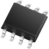
MCP79412T-I/ST Microchip Technology, MCP79412T-I/ST Datasheet - Page 10

MCP79412T-I/ST
Manufacturer Part Number
MCP79412T-I/ST
Description
Real Time Clock I2C GP RTCC 1Kb EE 64B SRAM EUI-64
Manufacturer
Microchip Technology
Series
-r
Type
Clock/Calendarr
Datasheet
1.MCP79412-ISN.pdf
(40 pages)
Specifications of MCP79412T-I/ST
Function
Clock/Calendar
Rtc Memory Size
64 Byte
Maximum Operating Temperature
+ 85 C
Minimum Operating Temperature
- 40 C
Rtc Bus Interface
I2C
Supply Current
1 uA
Features
Alarm, Leap Year, NVSRAM, Square Wave Output, Unique ID
Memory Size
64B
Time Format
HH:MM:SS (12/24 hr)
Date Format
YY-MM-DD-dd
Interface
I²C
Voltage - Supply
1.8 V ~ 5.5 V
Voltage - Supply, Battery
1.3 V ~ 5.5 V
Operating Temperature
-40°C ~ 85°C
Mounting Type
Surface Mount
Package / Case
8-TSSOP (0.173", 4.40mm Width)
Lead Free Status / RoHS Status
Lead free / RoHS Compliant
MCP7941X
4.0
The MCP7941x family is a highly integrated RTCC. On-
board time and date counters are driven from a low-
power oscillator to maintain the time and date. An
integrated V
the time and date and also the contents of the SRAM
during a V
4.1
The RTCC registers are contained in addresses
0x00h-0x1fh. 64 bytes of user-accessable SRAM are
located in the address range 0x20-0x5f. The SRAM
memory is a separate block from the RTCC control
and Configuration registers. All SRAM locations are
battery-backed-up during a V
locations are not accessible, MCP7941X will noACK
after the address byte if the address is out of range, as
shown in the shaded region of the memory map in
Figure
• Addresses 0x00h-0x06h are the RTCC Time and
• Incorrect data can appear in the Time and Date
• Addresses 0x07h-0x09h are the device Configu-
• Addresses 0x0Ah-0x10h are the Alarm 0 regis-
• Addresses 0x11h-0x17h are the same as 0x0Bh-
• Addresses 0x18h-0x1Fh are used for the time-
The detailed memory map is shown in
The shaded areas are not implemented and read as ‘0’.
No error checking is provided when loading time and
date registers.
DS22266C-page 10
Date registers. These are read/write registers.
Care must be taken when writing to these regis-
ters with the oscillator running.
registers if a write is attempted during the time
frame where these internal registers are being
incremented. The user can minimize the likeli-
hood of data corruption by ensuring that any
writes to the Time and Date registers occur before
the contents of the second register reach a value
of 0x59H.
ration, Calibration and ID Unlock registers.
ters. These are used to set up the Alarm 0, the
Interrupt polarity and the Alarm 0 Compare.
0x11h but are used for Alarm 1.
stamp feature.
4-1.
RTCC FUNCTIONALITY
RTCC MEMORY MAP
CC
CC
power failure.
switch enables the device to maintain
CC
power fail. Unused
Table
4-1.
FIGURE 4-1:
0x0A
0x00
0x06
0x07
0x09
0x10
0x11
0x17
0x18
0x1F
0x20
0x5F
0x60
0xFF
Configuration and Calibration
2010-2011 Microchip Technology Inc.
MEMORY MAP
SRAM (64 Bytes)
Time and Date
Time-Stamp
Alarm 0
Alarm 1


