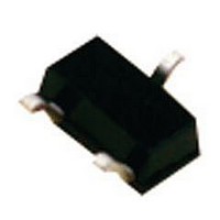
SI1021R-T1-E3 Vishay, SI1021R-T1-E3 Datasheet - Page 4

SI1021R-T1-E3
Manufacturer Part Number
SI1021R-T1-E3
Description
MOSFET P-CH 60V 190MA SC-75A
Manufacturer
Vishay
Series
TrenchFET®r
Datasheet
1.SI1021R-T1-E3.pdf
(5 pages)
Specifications of SI1021R-T1-E3
Transistor Polarity
P-Channel
Fet Type
MOSFET P-Channel, Metal Oxide
Fet Feature
Logic Level Gate
Rds On (max) @ Id, Vgs
4 Ohm @ 500mA, 10V
Drain To Source Voltage (vdss)
60V
Current - Continuous Drain (id) @ 25° C
190mA
Vgs(th) (max) @ Id
3V @ 250µA
Gate Charge (qg) @ Vgs
1.7nC @ 15V
Input Capacitance (ciss) @ Vds
23pF @ 25V
Power - Max
250mW
Mounting Type
Surface Mount
Package / Case
SC-75-3, SOT-416, EMT3, 3-SSMini
Minimum Operating Temperature
- 55 C
Configuration
Single
Resistance Drain-source Rds (on)
8 Ohms
Forward Transconductance Gfs (max / Min)
80 mS
Drain-source Breakdown Voltage
- 60 V
Gate-source Breakdown Voltage
+/- 20 V
Continuous Drain Current
- 190 mA
Power Dissipation
250 mW
Maximum Operating Temperature
+ 150 C
Mounting Style
SMD/SMT
Continuous Drain Current Id
-190mA
Drain Source Voltage Vds
-60V
On Resistance Rds(on)
5ohm
Rds(on) Test Voltage Vgs
-10V
Threshold Voltage Vgs Typ
-3V
Lead Free Status / RoHS Status
Lead free / RoHS Compliant
Lead Free Status / RoHS Status
Lead free / RoHS Compliant, Lead free / RoHS Compliant
Other names
SI1021R-T1-E3TR
Si1021R
Vishay Siliconix
TYPICAL CHARACTERISTICS (T
Vishay Siliconix maintains worldwide manufacturing capability. Products may be manufactured at one of several qualified locations. Reliability data for Silicon
Technology and Package Reliability represent a composite of all qualified locations. For related documents such as package/tape drawings, part marking, and
reliability data, see
www.vishay.com
4
1000
- 0.0
- 0.1
- 0.2
- 0.3
100
0.5
0.4
0.3
0.2
0.1
10
1
0.01
0.00
- 50
0.1
Threshold Voltage Variance Over Temperature
2
1
www.vishay.com/ppg?71410.
10
V
- 25
-4
Source-Drain Diode Forward Voltage
GS
T
Duty Cycle = 0.5
0.2
0.1
0.05
0.02
J
= 0 V
0.3
= 125 °C
V
SD
T
0
I
J
D
- Junction Temperature (°C)
- Source-to-Drain Voltage (V)
= 250 µA
25
0.6
10
Single Pulse
-3
50
Normalized Thermal Transient Impedance, Junction-to-Ambient
T
0.9
J
75
T
= - 55 °C
J
= 25 °C
A
100
= 25 °C, unless otherwise noted)
10
1.2
-2
125
1.5
150
Square Wave Pulse Duration (s)
10
-1
2.5
1.5
0.5
10
8
6
4
2
0
3
2
1
0
0.01
1
0
On-Resistance vs. Gate-Source Voltage
Single Pulse Power, Junction-to-Ambient
0.1
2
V
GS
I
D
- Gate-to-Source Voltage (V)
= 200 mA
1
Notes:
1. Duty Cycle, D =
2. Per Unit Base = R
3. T
4. Surface Mounted
0
P
DM
4
1
JM
- T
Time (s)
t
A
1
S10-2687-Rev. F, 22-Nov-10
T
= P
A
t
2
Document Number: 71410
= 25 °C
DM
6
Z
10
thJA
thJA
100
I
t
t
1
2
D
(t)
= 500 mA
= 500 °C/W
8
100
6
0
0
600
10


