NTJD4105CT2 ON Semiconductor, NTJD4105CT2 Datasheet
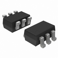
MOSFET N/P-CHAN COMPL SOT-363

NTJD4105CT2

Manufacturer Part Number
NTJD4105CT2
Description
MOSFET N/P-CHAN COMPL SOT-363
Manufacturer
ON Semiconductor
Datasheet

Specifications of NTJD4105CT2

Fet Type
N and P-Channel
Fet Feature
Logic Level Gate
Rds On (max) @ Id, Vgs
375 mOhm @ 630mA, 4.5V
Drain To Source Voltage (vdss)
20V, 8V
Current - Continuous Drain (id) @ 25° C
630mA, 775mA
Vgs(th) (max) @ Id
1.5V @ 250µA
Gate Charge (qg) @ Vgs
3nC @ 4.5V
Input Capacitance (ciss) @ Vds
46pF @ 20V
Power - Max
270mW
Mounting Type
Surface Mount
Package / Case
SC-70-6, SC-88, SOT-363
Lead Free Status / RoHS Status
Contains lead / RoHS non-compliant

Available stocks

Company
Part Number
Manufacturer
Quantity
Price
Part Number:
NTJD4105CT2G
Manufacturer:
ON
Quantity:
30 000
Part Number:
NTJD4105CT2G
Manufacturer:
ON/安森美
Quantity:
20 000
Part Number:
NTJD4105CT2G
0
NTJD4105C
Small Signal MOSFET
20 V / −8.0 V, Complementary,
+0.63 A / −0.775 A, SC−88
Features
Applications
Stresses exceeding Maximum Ratings may damage the device. Maximum
Ratings are stress ratings only. Functional operation above the Recommended
Operating Conditions is not implied. Extended exposure to stresses above the
Recommended Operating Conditions may affect device reliability.
1. Surface mounted on FR4 board using 1 oz Cu area = 0.9523 in sq.
© Semiconductor Components Industries, LLC, 2006
March, 2006 − Rev. 2
MAXIMUM RATINGS
THERMAL RESISTANCE RATINGS (Note 1)
Drain−to−Source Voltage
Gate−to−Source Voltage
Continuous Drain Current
Pulsed Drain Current
Power Dissipation − Steady State
Operating Junction and Storage Temperature
Source Current (Body Diode)
Lead Temperature for Soldering Purposes
Junction−to−Ambient
Junction−to−Lead (Drain)
Complementary N and P Channel Device
Leading −8.0 V Trench for Low R
ESD Protected Gate − ESD Rating: Class 1
SC−88 Package for Small Footprint (2 x 2 mm)
Pb−Free Packages are Available
DC−DC Conversion
Load/Power Switching
Single or Dual Cell Li−Ion Battery Supplied Devices
Cell Phones, MP3s, Digital Cameras, PDAs
− Steady State
(Based on R
− Steady State
(Based on R
(Based on R
(Based on R
(1/8” from case for 10 s)
– Steady State
– Steady State
qJA
qJL
qJA
qJL
Parameter
)
)
)
)
(T
J
N−Ch
P−Ch
N−Ch
P−Ch
= 25°C unless otherwise noted)
T
T
T
T
T
T
T
T
T
T
T
T
tp ≤ 10 ms
A
A
A
A
A
A
A
A
A
A
A
A
N−Ch
P−Ch
N−Ch
P−Ch
N−Ch
P−Ch
Max
Max
= 25°C
= 85°C
= 25°C
= 85°C
= 25°C
= 85°C
= 25°C
= 85°C
= 25°C
= 85°C
= 25°C
= 85°C
Typ
Typ
DS(on)
Performance
Symbol
V
T
R
R
V
I
P
T
DSS
STG
T
DM
I
I
qJA
qJL
GS
D
S
J
D
L
,
−0.775
−0.558
−0.775
−55 to
Value
−8.0
±8.0
0.63
0.46
0.91
0.65
−1.1
−0.8
±1.2
0.27
0.14
0.55
0.29
0.63
±12
150
260
400
460
194
226
20
1
°C/W
Unit
°C
°C
W
V
V
A
A
A
See detailed ordering and shipping information in the package
dimensions section on page 7 of this data sheet.
V
N−Ch 20 V
P−Ch −8.0 V
SC−88/SOT−363
(BR)DSS
CASE 419B
(Note: Microdot may be in either location)
G
D
STYLE 28
S
1
1
2
ORDERING INFORMATION
TC
M
G
1
1
2
3
http://onsemi.com
SC−88 (6−LEADS)
0.22 W @ −4.5 V
0.32 W @ −2.5 V
0.51 W @ −1.8 V
0.29 W @ 4.5 V
0.36 W @ 2.5 V
R
= Device Code
= Date Code
= Pb−Free Package
DS(on)
SOT−363
Top View
MARKING DIAGRAM &
PIN ASSIGNMENT
Publication Order Number:
6
1
TYP
D1 G2 S2
S1 G1 D2
TC M G
G
6
5
4
NTJD4105C/D
−0.775 A
I
0.63 A
D
Max
D
G
S
2
1
2

Related parts for NTJD4105CT2

NTJD4105CT2 Summary of contents

Page 1

NTJD4105C Small Signal MOSFET −8.0 V, Complementary, +0. −0.775 A, SC−88 Features • Complementary N and P Channel Device • Leading −8.0 V Trench for Low R DS(on) • ESD Protected Gate − ESD Rating: ...

Page 2

ELECTRICAL CHARACTERISTICS Parameter Symbol OFF CHARACTERISTICS Drain−to−Source V (BR)DSS Breakdown Voltage Drain−to−Source Breakdown V (BR)DSS Voltage Temperature Coeffi cient Zero Gate Voltage Drain Cur- I DSS rent Gate−to−Source I GSS Leakage Current ON CHARACTERISTICS (Note 2) Gate ...

Page 3

TYPICAL N−CHANNEL PERFORMANCE CURVES 0.8 0.6 0.4 0 DRAIN−TO−SOURCE VOLTAGE (VOLTS) DS Figure 1. On−Region Characteristics 0.7 ...

Page 4

TYPICAL N−CHANNEL PERFORMANCE CURVES 5 Q G(TOT 0.2 0.4 0.6 0 TOTAL GATE CHARGE (nC) g Figure 7. Gate−to−Source and Drain−to−Source Voltage vs. Total Charge (T J ...

Page 5

TYPICAL P−CHANNEL PERFORMANCE CURVES 1 −4 −2 −2 1.2 − 0.8 0.6 0.4 0 −V , DRAIN−TO−SOURCE VOLTAGE (VOLTS) DS Figure 9. On−Region Characteristics ...

Page 6

TYPICAL P−CHANNEL PERFORMANCE CURVES 5 Q G(TOT 0.4 0.8 1.2 1 TOTAL GATE CHARGE (nC) g Figure 15. Gate−to−Source and Drain−to−Source Voltage vs. Total Charge (T J ...

Page 7

... ORDERING INFORMATION Device NTJD4105CT1 NTJD4105CT1G NTJD4105CT2 NTJD4105CT2G NTJD4105CT4 NTJD4105CT4G †For information on tape and reel specifications, including part orientation and tape sizes, please refer to our Tape and Reel Packaging Specifications Brochure, BRD8011/D. Package SOT−363 SOT−363 (Pb−Free) SOT−363 SOT−363 (Pb− ...

Page 8

... Pb−Free strategy and soldering details, please download the ON Semiconductor Soldering and Mounting Techniques Reference Manual, SOLDERRM/D. ON Semiconductor and are registered trademarks of Semiconductor Components Industries, LLC (SCILLC). SCILLC reserves the right to make changes without further notice to any products herein ...

Related keywords