MMVL409T1 ON Semiconductor, MMVL409T1 Datasheet

Varactor Diodes 20V 26pF

MMVL409T1

Manufacturer Part Number
MMVL409T1
Description
Varactor Diodes 20V 26pF
Manufacturer
ON Semiconductor
Datasheet

Specifications of MMVL409T1

Capacitance
26 pF
Reverse Voltage
20 V
Termination Style
SMD/SMT
Applications Frequency Range
VHF
Configuration
Single
Maximum Operating Temperature
+ 150 C
Minimum Tuning Ratio
1.5
Mounting Style
SMD/SMT
Tuning Ratio Test Condition
3 / 8
Package / Case
SOD-323-2
Lead Free Status / RoHS Status
Lead free / RoHS Compliant
MMVL409T1
Silicon Tuning Diode
applications. They provide solid−state reliability in replacement of
mechanical tuning methods.
Features
Maximum ratings are those values beyond which device damage can occur.
Maximum ratings applied to the device are individual stress limit values (not
normal operating conditions) and are not valid simultaneously. If these limits are
exceeded, device functional operation is not implied, damage may occur and
reliability may be affected.
1. FR−4 Minimum Pad
MAXIMUM RATINGS
THERMAL CHARACTERISTICS
© Semiconductor Components Industries, LLC, 2006
February, 2006 − Rev. 3
Continuous Reverse Voltage
Peak Forward Current
Total Device Dissipation FR−5 Board,
T
Derate above 25°C
Thermal Resistance, Junction−to−Ambient
Junction and Storage Temperature
These devices are designed for general frequency control and tuning
A
High Q with Guaranteed Minimum Values at VHF Frequencies
Controlled and Uniform Tuning Ratio
Surface Mount Package
Pb−Free Package is Available
= 25°C (Note 1)
Characteristic
Rating
Preferred Device
Symbol
Symbol
T
R
J
V
P
, T
I
qJA
F
R
D
stg
Value
Max
1.57
200
200
635
150
20
1
mW/°C
mAdc
°C/W
Unit
Unit
Vdc
mW
°C
†For information on tape and reel specifications,
Preferred devices are recommended choices for future use
and best overall value.
MMVL409T1
MMVL409T1G
including part orientation and tape sizes, please
refer to our Tape and Reel Packaging Specifications
Brochure, BRD8011/D.
*Date Code orientation may vary depending
Device
upon manufacturing location.
(Note: Microdot may be in either location)
CAPACITANCE DIODE
VOLTAGE VARIABLE
ORDERING INFORMATION
X5
M
G
CATHODE
MARKING DIAGRAM
http://onsemi.com
1
= Device Code
= Date Code*
= Pb−Free Package
SOD−323 3000 / Tape & Reel
SOD−323
(Pb−Free)
1
Package
CASE 477
SOD−323
PLASTIC
STYLE 1
Publication Order Number:
X5 M G
G
ANODE
2
3000 / Tape & Reel
2
Shipping
MMVL409T1/D

Related parts for MMVL409T1

MMVL409T1 Summary of contents

Page 1

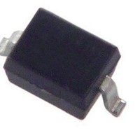
... STYLE 1 MARKING DIAGRAM Device Code M = Date Code Pb−Free Package (Note: Microdot may be in either location) upon manufacturing location. ORDERING INFORMATION † Device Package Shipping SOD−323 3000 / Tape & Reel SOD−323 3000 / Tape & Reel (Pb−Free) Publication Order Number: MMVL409T1/D ...

Page 2

... Vdc R 2.0 1.0 0.6 0.2 0.1 0.06 0.02 0.01 0.006 0.002 0.001 −60 −40 −20 0 +20 + AMBIENT TEMPERATURE (°C) A Figure 3. Leakage Current MMVL409T1 (T = 25°C unless otherwise noted) A Symbol V (BR Diode Capacitance 3.0 Vdc 1.0 MHz R pF Min Nom Max measured at 8 Vdc ...

Page 3

... E 1.15 1.25 1.35 0.045 0.049 0.053 L 0.08 0.003 H 2.30 2.50 2.70 0.090 0.098 0.105 E STYLE 1: PIN 1. CATHODE 2. ANODE 0.83 ON Semiconductor Website: http://onsemi.com Order Literature: http://www.onsemi.com/litorder For additional information, please contact your local Sales Representative. MMVL409T1/D ...

Related keywords