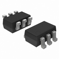
NTJD1155L
Power MOSFET
8 V, +1.3 A, High Side Load Switch with
Level−Shift, P−Channel SC−88
package. This device is particularly suited for portable electronic
equipment where low control signals, low battery voltages and high
load currents are needed. The P−Channel device is specifically
designed as a load switch using ON Semiconductor state−of−the−art
trench technology. The N−Channel, with an external resistor (R1),
functions as a level−shift to drive the P−Channel. The N−Channel
MOSFET has internal ESD protection and can be driven by logic
signals as low as 1.5 V. The NTJD1155L operates on supply lines from
1.8 to 8.0 V and can drive loads up to 1.3 A with 8.0 V applied to both
V
Features
•
•
•
•
•
•
•
Stresses exceeding Maximum Ratings may damage the device. Maximum
Ratings are stress ratings only. Functional operation above the Recommended
Operating Conditions is not implied. Extended exposure to stresses above the
Recommended Operating Conditions may affect device reliability.
1. Surface−mounted on FR4 board using 1 inch sq pad size
© Semiconductor Components Industries, LLC, 2007
March, 2007 − Rev. 4
MAXIMUM RATINGS
THERMAL CHARACTERISTICS
Input Voltage (V
ON/OFF Voltage (V
Continuous Load Current
(Note 1)
Power Dissipation
(Note 1)
Pulsed Load Current
Operating Junction and Storage Temperature
Source Current (Body Diode)
ESD Rating, MIL−STD−883D HBM
(100 pF, 1.5 kW)
Lead Temperature for Soldering Purposes
(1/8″ from case for 10 s)
Junction−to−Ambient – Steady State (Note 1)
Junction−to−Foot – Steady State (Note 1)
IN
The NTJD1155L integrates a P and N−Channel MOSFET in a single
Extremely Low R
Level Shift MOSFET is ESD Protected
Low Profile, Small Footprint Package
V
ON/OFF Range 1.5 to 8.0 V
ESD Rating of 3000 V
Pb−Free Package is Available
(Cu area = 1.127 in sq [1 oz] including traces).
IN
and V
Range 1.8 to 8.0 V
ON/OFF.
Characteristic
DSS
Rating
GS
, P−Ch)
DS(on)
, N−Ch)
(T
J
Steady
Steady
State
State
= 25°C unless otherwise noted)
P−Channel Load Switch MOSFET
t
p
= 10 ms
T
T
T
T
A
A
A
A
= 25°C
= 85°C
= 25°C
= 85°C
V
Symbol
Symbol
ON/OFF
T
ESD
R
R
V
I
T
P
STG
T
LM
I
I
qJA
qJF
IN
L
S
J
D
L
,
−55 to
Value
±1.3
±0.9
0.40
0.20
±3.9
−0.4
Max
150
260
320
220
8.0
8.0
3.0
1
°C/W
Unit
Unit
kV
°C
°C
W
V
V
A
A
A
†For information on tape and reel specifications,
NTJD1155LT1
NTJD1155LT1G
TB
M
G
(Note: Microdot may be in either location)
including part orientation and tape sizes, please
refer to our Tape and Reel Packaging Specification
Brochure, BRD8011/D.
V
(BR)DSS
8.0 V
Device
= Device Code
= Date Code
= Pb−Free Package
1
ORDERING INFORMATION
SIMPLIFIED SCHEMATIC
4
6
5
http://onsemi.com
http://onsemi.com
PIN ASSIGNMENT
CASE 419B
D1/G2
(SOT−363)
STYLE 30
130 mW @ −4.5 V
170 mW @ −2.5 V
260 mW @ −1.8 V
SC−88
S1
R
(Pb−Free)
6
1
Package
DS(on)
SC−88
SC−88
G1
D2
Publication Order Number:
5
2
TYP
1
S2
4
3
D2
Q2
Q1
3000/Tape & Reel
3000/Tape & Reel
1
2,3
Shipping
MARKING
DIAGRAM
NTJD1155L/D
TB M G
I
D
±1.3 A
G
MAX
†


