NTJD4152PT1G ON Semiconductor, NTJD4152PT1G Datasheet - Page 2
NTJD4152PT1G
Manufacturer Part Number
NTJD4152PT1G
Description
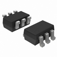
MOSFET 2P-CH 20V 880MA SOT-363
Manufacturer
ON Semiconductor
Type
Small Signalr
Specifications of NTJD4152PT1G
Fet Type
2 P-Channel (Dual)
Fet Feature
Logic Level Gate
Rds On (max) @ Id, Vgs
260 mOhm @ 880mA, 4.5V
Drain To Source Voltage (vdss)
20V
Current - Continuous Drain (id) @ 25° C
880mA
Vgs(th) (max) @ Id
450mV @ 250µA
Gate Charge (qg) @ Vgs
2.2nC @ 4.5V
Input Capacitance (ciss) @ Vds
155pF @ 20V
Power - Max
272mW
Mounting Type
Surface Mount
Package / Case
SC-70-6, SC-88, SOT-363
Configuration
Dual
Transistor Polarity
P-Channel
Resistance Drain-source Rds (on)
0.26 Ohm @ 4.5 V
Forward Transconductance Gfs (max / Min)
3 S
Drain-source Breakdown Voltage
20 V
Gate-source Breakdown Voltage
+/- 12 V
Continuous Drain Current
0.88 A
Power Dissipation
272 mW
Maximum Operating Temperature
+ 150 C
Mounting Style
SMD/SMT
Minimum Operating Temperature
- 55 C
Module Configuration
Dual
Continuous Drain Current Id
880mA
Drain Source Voltage Vds
-20V
On Resistance Rds(on)
215mohm
Rds(on) Test Voltage Vgs
-4.5V
Rohs Compliant
Yes
Number Of Elements
2
Polarity
P
Channel Mode
Enhancement
Drain-source On-res
0.26Ohm
Drain-source On-volt
20V
Gate-source Voltage (max)
±12V
Operating Temp Range
-55C to 150C
Operating Temperature Classification
Military
Mounting
Surface Mount
Pin Count
6
Package Type
SC-88
Lead Free Status / RoHS Status
Lead free / RoHS Compliant
Other names
NTJD4152PT1GOSTR
Available stocks
Company
Part Number
Manufacturer
Quantity
Price
Company:

Part Number:
NTJD4152PT1G
Manufacturer:
ON
Quantity:
36 000
Company:
Part Number:
NTJD4152PT1G
Manufacturer:
ON
Quantity:
3 000
Company:
Part Number:
NTJD4152PT1G
Manufacturer:
ON
Quantity:
30 000
Part Number:
NTJD4152PT1G
Manufacturer:
ON/安森美
Quantity:
20 000


3. V
4. Surge current waveform per Figure 5.
5. For test procedure see Figures 3 and 4 and Application Note AND8307/D.
ELECTRICAL CHARACTERISTICS
(T
ELECTRICAL CHARACTERISTICS
NSQA6V8AW5T2
NSQA12VAW5T2
*See Application Note AND8308/D for detailed explanations of
Breakdown Voltage (I
Leakage Current (V
Clamping Voltage 1 (I
Maximum Peak Pulse Current (Note 4)
Junction Capacitance − (V
Clamping Voltage − Per IEC61000−4−2
Breakdown Voltage (I
Leakage Current (V
Zener Impedence (I
Clamping Voltage 1 (I
Maximum Peak Pulse Current (Note 4)
Junction Capacitance − (V
Clamping Voltage − Per IEC61000−4−2 (Note 5)
Symbol
A
datasheet parameters.
V
V
P
= 25°C unless otherwise noted)
I
RWM
V
V
I
PP
I
I
C
BR
BR
R
T
F
pk
C
F
is measured at pulse test current I
Maximum Reverse Peak Pulse Current
Clamping Voltage @ I
Peak Power Dissipation
Capacitance @ V
Working Peak Reverse Voltage
Maximum Reverse Leakage Current @ V
Breakdown Voltage @ I
Test Current
Forward Current
Forward Voltage @ I
RWM
RWM
T
T
T
= 5 mA)
PP
PP
− (V
= 1 mA) (Note 3)
= 5 mA) (Note 3)
= 1.6 A) (Note 4)
= 0.9 A) (Note 4)
= 5.0 V)
= 9.0 V)
R
R
R
= 0 V, f = 1 MHz)
= 3.0 V, f = 1 MHz)
= 0 V, f = 1 MHz)
R
Characteristic
= 0 and f = 1.0 MHz
Parameter
F
PP
T
(T
T
.
A
= 25°C unless otherwise noted)
RWM
http://onsemi.com
2
Symbol
V
V
V
I
I
V
V
V
V
C
Z
C
I
I
PP
PP
BR
BR
R
R
C
C
C
C
C
Z
J
J
V
BR
V
RWM
11.4
Min
6.4
−
−
−
−
−
−
−
−
−
−
Uni−Directional
I
Figures 1 and 2
Figures 1 and 2
F
I
I
I
I
R
T
PP
12.0
Typ
6.8
6.7
12
V
−
−
−
−
−
−
−
−
F
Max
12.7
0.05
7.1
1.0
1.6
9.5
0.9
13
15
30
23
15
V
Unit
mA
mA
pF
pF
W
V
V
A
V
V
V
A
V
Related parts for NTJD4152PT1G
Image
Part Number
Description
Manufacturer
Datasheet
Request
R

Part Number:
Description:
ON Semiconductor [VOLTAGE REGULATOR]
Manufacturer:
ON Semiconductor
Datasheet:
Part Number:
Description:
357-036-542-201 CARDEDGE 36POS DL .156 BLK LOPRO
Manufacturer:
ON Semiconductor
Datasheet:
Part Number:
Description:
357-036-542-201 CARDEDGE 36POS DL .156 BLK LOPRO
Manufacturer:
ON Semiconductor
Datasheet:
Part Number:
Description:
357-036-542-201 CARDEDGE 36POS DL .156 BLK LOPRO
Manufacturer:
ON Semiconductor
Datasheet:
Part Number:
Description:
357-036-542-201 CARDEDGE 36POS DL .156 BLK LOPRO
Manufacturer:
ON Semiconductor
Datasheet:
Part Number:
Description:
357-036-542-201 CARDEDGE 36POS DL .156 BLK LOPRO
Manufacturer:
ON Semiconductor
Datasheet:
Part Number:
Description:
357-036-542-201 CARDEDGE 36POS DL .156 BLK LOPRO
Manufacturer:
ON Semiconductor
Datasheet:
Part Number:
Description:
357-036-542-201 CARDEDGE 36POS DL .156 BLK LOPRO
Manufacturer:
ON Semiconductor
Datasheet:
Part Number:
Description:
357-036-542-201 CARDEDGE 36POS DL .156 BLK LOPRO
Manufacturer:
ON Semiconductor
Datasheet:
Part Number:
Description:
357-036-542-201 CARDEDGE 36POS DL .156 BLK LOPRO
Manufacturer:
ON Semiconductor
Datasheet:
Part Number:
Description:
357-036-542-201 CARDEDGE 36POS DL .156 BLK LOPRO
Manufacturer:
ON Semiconductor
Datasheet:
Part Number:
Description:
Manufacturer:
ON Semiconductor
Datasheet:
Part Number:
Description:
Manufacturer:
ON Semiconductor
Datasheet:
Part Number:
Description:
Manufacturer:
ON Semiconductor
Datasheet: